- A contact serves as an interface through which the semiconductor
device interacts with its environment. It is needed to apply
excitation to the device and to extract signal from it.
- A contact should perform this task with the least alteration
of the device characteristics.
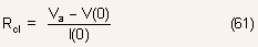
A Figure-of-Merit that is a measure of this characteristics
is the specific contact resistance defined as :
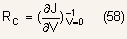
- The derivative is defined at 0 = V because no voltage should
ideally drop across the junction.
- Contacts are formed by depositing metal over the semiconductor.
However, a straightforward deposition of a metal such as Aluminum
on Silicon will yield only a Schottky diode whose specific contact
resistance will be very high.
Example 5.1 : Determine the specific contact resistance of
a contact formed by simply depositing Aluminum on N-type Silicon
of doping

.
Such a contact will be a Schottky contact which will obey the current
equation:
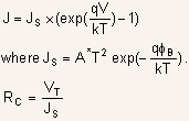
Differentiation
of the above equation gives:
For a barrier height of 0.7 eV,

Example 5.2 : Such a large contact resistance is completely
unacceptable. To understand what would constitute a good value for
the contact resistance, let us consider the example of a PN junction
diode with a contact area of

.
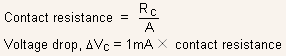
Calculate the contact resistance for contact resistivities of
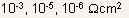
(b) Calculate also the voltage drop across the contact for a current
of 1mA.
(c) Determine the factor by which the diode’s characteristics
will get modified as a result of this voltage drop.
Solution :
Because of the exponential nature of diode’s characteristics
(~exp(qV/kT)), the modification factor will be

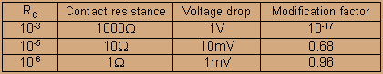
The table below shows the resistance due to contact, voltage drop
across it and the modification of diode’s characteristics for
various values of specific contact resistances.
- This example illustrates that specific contact resistance
better than
 is
required.
is
required.
- This implies that through suitable modifications, the specific
contact resistance of the metal-semiconductor junction has to
be lowered from a value of
 ,
a nine orders of magnitude reduction!
,
a nine orders of magnitude reduction!
- This tremendous feat is achieved by increasing the tunneling
current in the diode. Normally, this current for doping less
than
 is
negligible but as the doping is increased, it becomes increasingly
important.
is
negligible but as the doping is increased, it becomes increasingly
important.
- The tunneling probability depends exponentially on the height
and the thickness of the barrier:
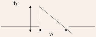
- The transmission probability for the triangular approx. of
the barrier is given by:
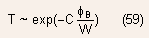
As doping is increased, the thickness W of the barrier decreases,
increasing the transmission coefficient and thereby the current.
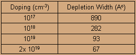
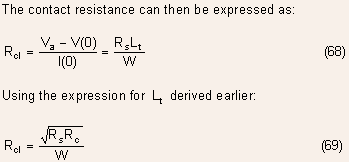
Example 5.3 : Determine depletion widths for Schottky barrier
diodes made on N-type Silicon with doping values of
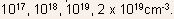
Assume that barrier height is 0.7eV .Using the expressions derived
earlier, we obtain
The table above shows that for doping

,
the barrier width is very narrow making tunneling very significant.
Since the depletion width goes as

the
specific contact resistance, being inversely proportional to transmission
probability when tunneling becomes the dominant current conduction
mechanism can be expressed as:
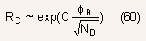
The expression above shows that a small barrier height and high
doping level is required to obtain good contacts.
For

,
the specific contact resistance is determined entirely by the tunneling
process and decreases rapidly as doping is further increased.
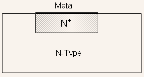
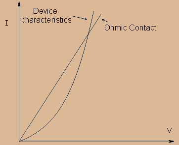
As a result, a contact to an N or P-type semiconductor is made by
first heavily doping the semiconductor region under the contact
and then depositing a metal such as aluminum over it as illustrated
in the Figure.
Although, a contact like this is a good Ohmic contact for electrons,
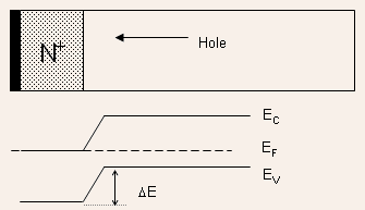
it is however, a poor contact for holes! The reasons for this can
be understood by considering a 1-D abstraction of the above schematic
as shown below:
The holes travelling from the

see
a barrier of height

which
obstructs their flow to the contact. As a result, these contacts
are called reflecting contacts for the minority carriers.
The current flow under the contacts was assumed to be perpendicular
for the cases discussed so far. There are contacts however, where
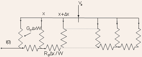
the current flow is lateral as illustrated by the Figure below:
The contact resistance is now determined not only by the specific
resistance of the contact but also by the sheet resistance of the
semiconductor layer underneath.
These contacts can be modeled using a transmission line model described
below:
Definitions:
-

is
the sheet resistance of the semiconductor underneath the contact
so that

represents
the incremental series resistance, where W is the width of the contact
perpendicular to the plane of the diagram.
-

where,
R
c is the specific contact resistance so that

represents
the conductance of the vertical section
Contact resistance:
The following set of equations can be easily written for the transmission
line representation
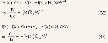
The equations above lead to the following differential equation:
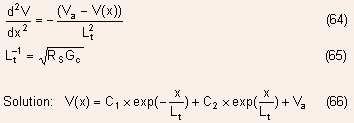
For simplicity we shall take a contact that is long enough in the
x-direction and assume that

.
If this the case then

Using
the other boundary condition that I at x=0 is I(0) , we obtain
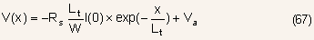
The contact resistance in this case scales with only the width of
the contact and not its area as for the earlier case. It is therefore
specified as

in
units of

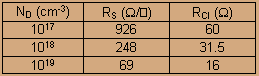
Example 5.4 : Determine the lateral contact resistance for
a contact of area

specific
contact resistance of

and
a set of doping values given below. The semiconductor under the
contact is N-type of thickness 1micro metre.
 Solution
 : The sheet resistance of the semiconductor is given
by the expression:

,where
t is the thickness of the semiconductor. This equation along with
Eq. (69) gives the following values for contact resistance:
The example illustrates that very low values of sheet resistance
are required to obtain a small lateral contact resistance and even
then it is much higher that the contact resistance

for the above example) when the current flow under the contact is
vertical.
- Thus a high doping under the semiconductor is needed to lower
both the specific contact resistance as well as the sheet resistance.
- The importance of Ohmic contact increases as current through
the device increases and as the dimensions of the device are
scaled to improve its performance.
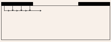
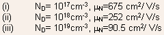
- Since characteristics of most semiconductor devices such as
diodes, BJTs, MOSFETs etc are non-linear, while that of a contact
linear, the voltage drop across the contact would tend to become
comparable and even greater at higher currents as illustrated
by the Figure above.
- To understand the increased importance of contact resistance
as the device is scaled down, let us first consider a BJT and
then a MOSFET.
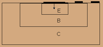
In a BJT let us take the emitter resistance. The current flow
through the semiconductor under the contact is perpendicular
as illustrated by the Figure below:
Since the I-V characteristics of the emitter-base junction is
exponential in nature  ,
the voltage drop
,
the voltage drop  should
be much smaller than the thermal voltage V
should
be much smaller than the thermal voltage V
Example 5.5 : For an emitter area of

,
specific contact resistivity of

determine the maximum value of emitter current before the contact
begins to make appreciable difference to the transistor’s characteristics.
Solution : Taking a maximum contact voltage drop of

so
that there is less than 10% change in transistor’s current,
we obtain
Suppose now the emitter area is scaled by a factor of 10, while
keeping the emitter current constant so as to improve the transistor’s
performance (which upto a limit improves as the collector current
density increases).
The voltage drop across the contact now becomes 50mV, which is very
significant!
If the voltage drop is to be maintained at the earlier 5mV level,
the specific contact resistance will have to be lowered to

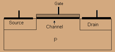
Consider now a MOSFET and the impact of the source contact resistance:
The current under the source flows laterally so that the expression

is
the contact resistance here. The role of the source resistance is
that it lowers the transconductance of the device
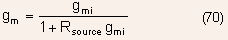
where

is
the transconductance of the transistor in the absence of a source
resistor. We would like

to
be as small as possible. A simplified expression for the transconductance
is
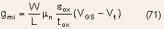
As the channel length and width are scaled by a factor K, the oxide
thickness is also reduced so that for a fixed supply voltage, the
transconductance increases in magnitude.The resistance due to the
contact however, increases by a factor K as the width is scaled.
Therefore, the product
would
become larger with scaling making it necessary to reduce the contact
resistance with scaling.
For the case, where the supply voltage is scaled also, the transconductance
may not increase but due to increase in contact resistance, the
problem persists though with lesser impact.
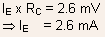
Example 5.6 : Determine the factor by which the transconductance
of a MOSFET is reduced as a result of voltage drop across the source
resistance . The MOSFET has the following characteristics:

The source contact has the following characteristics:

(b) Redo your calculations for

but
W/L = 10 as before. Assume that new ,

For
the contact assume that every thing is same except that

.
Solution : Using Eq.(70) and (71), we obtain

=
0.95
(b) As a result of scaling of channel length by a factor of 2, the
intrinsic transconductance will increase by a factor of 2 and the
source resistance will also increase by the same factor. As a result
the
product
becomes four times and
=
0.84 now.