- Almost all the metals form a junction with Silicon such that a barrier exists for the flow of electrons in N-type material and for holes in P-type material. We shall confine out attention to Schottky barriers on N-type semiconductors only
- Although the barrier exists for flow of electrons in both the directions (metal-to-semiconductor or semiconductor-to-metal), the nature of the barrier is different.
- While the barrier to flow of electrons from metal-to-semiconductor remains fixed, the barrier to flow of electrons from semiconductor-to-metal changes as a bias is applied across the junction.
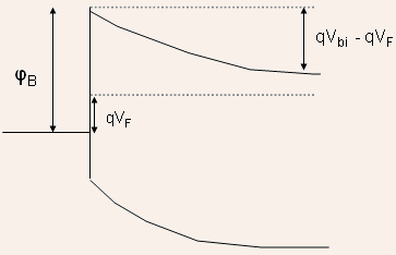
It can be seen from the Figure that the semiconductor-to-metal barrier is reduced by qVF.
In Forward bias, when metal is made positive with respect to the semiconductor, there should be a net flow of electrons towards the metal.The current in general can be expressed as:
Since the barrier to flow of electrons from the metal-to-semiconductor remains unchanged, so the component
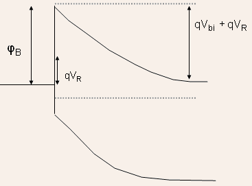
In this case, the barrier to electron flow into the metal has been increased making
Since the barrier to flow of electrons from the metal into the semiconductor remains the same,
Current Path from Ohmic Contact To Schottky Contact
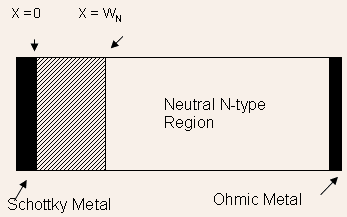
The flow of electrons from the backside Ohmic contact to the Schottky metal can be broken into three distinct parts:
- flow of electrons across the Ohmic contact and the neutral N-region
- flow of electrons across the depletion region
- flow of electrons across the Schottky metal-semiconductor interface
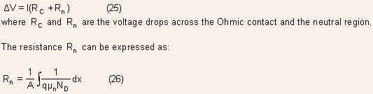
We normally want to keep the IR voltage drop as small as possible so that when Schottky diode is ON, the forward voltage drop is as small as possible.
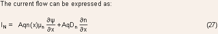
The current flow involves both drift and diffusion currents.
The two currents oppose each other with electrons tending to move towards the metal via diffusion and away from the metal via drift. In equilibrium, they cancel each other.
As a result of forward bias, the electric field gets reduced making the diffusion current exceed the drift current and causing a net flow of electrons towards the metal.
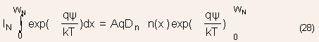
Using the relation
where V is the applied voltage and DV is the drop across the ohmic contact and neutral N-region.
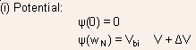
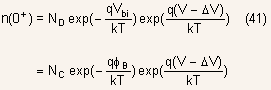
It is not clear as of now what the electron density at the interface should be.
The variation of voltage
The depletion width
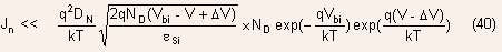
With the boundary conditions listed earlier and the expression for variation of potential across the depletion region, the current can be expressed as :
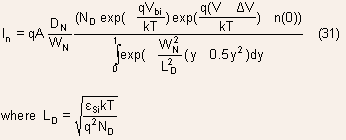
For typical values of doping and voltages
This allows the denominator of Eq. (31) to be simplified as
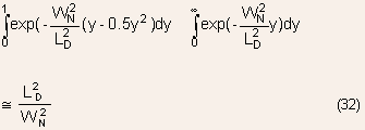
Eq.(31) can now be written as
- The expression for current can be obtained if the value of n(0) is known. For this we shall have to look at the transport across the metal-semiconductor interface.
- To begin with, we shall assume that the transport mechanism is predominantly thermionic emission and not tunneling
- Thermionic emission is one of the dominant mechanisms of current
flow across abrupt barriers as illustrated below:
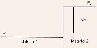
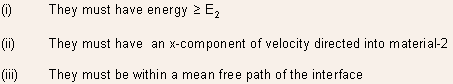
- There may be large number of electrons in material-1 but only a few can contribute to current flow and this number will increase as temperature is raised
- The electrons, which can contribute to current flow, must have the following characteristics:
- If the electrons are assumed to be moving randomly, then the current
due to flow of electrons from material-1 to material-2 can be written
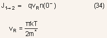
as:
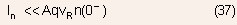
- VR is the average velocity of electrons in the positive x direction. Similarly, the flux of electrons towards materla-1 can be written as:
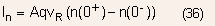
- The net electron current can therefore be expressed as
With this expression we can now determine the I-V characteristics of the Schottky barrier diode.
| There can be two extreme cases: | |
| (i) current is determined primarily by
drift-diffusion flow of electrons across the depletion region (ii) current is determined primarily by thermionic emission. |
|
- The first case implies that the bottleneck to current flow is drift
diffusion across the depletion region. If this is true then the current
should be much smaller than either the left or the right flux of electrons
in the expression for thermionic current.
Since the metal can be assumed to remain at equilibrium despite the current flow:
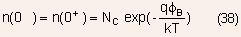
Since the current densities are most of the time several orders of magnitude larger than this, the first extreme case will not hold true at all.
- Let us take the other extreme case. In this case, if drift-diffusion
is not a bottleneck, then the net current should be much less than
either of the two terms in the expression given by Eq.(33)
Substitution of typical values shows that this condition is indeed satisfied, so that it can be assumed that the current is determined primarily by thermionic emission.
The above inequality along with Eq. (33) also allows us to write:
The net current density through the diode can be written as
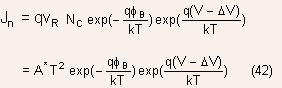
where A* is known as the Richardson constant and has a value of for
N-type Silicon.
for
N-type Silicon.
- A similar expression holds for current flow in P-type Schottky
barriers for which the Richardson constant is
 for
Silicon.
for
Silicon.
Example 2.1 : For an N-type Schottky diode with barrier height of 0.7eV, determine the forward on voltage for a forward current density of
Solution : Using Eq. (42) and assuming negligible voltage drop across neutral P-region we obtain VON = 0. 195 Volts, which is about 300mV lower that PN junction diode,has a reverse saturation current of
Example 2.2 : Repeat Q.2.1 for a P-type Schottky barrier diode with barrier height of 0.58eV.
Solution : Using Eq. (42) and assuming negligible voltage drop across neutral P-region at the low current density value, we obtain VON = 0. 195 Volts, which is about 400mV lower that PN junction diode. All nice things however, come at a price!
Example 2.3 : Calculate the reverse saturation currents for N and P Schottky diodes discussed above and compare it with a typical value of
Using the expressions derived earlier, the reverse leakage current turns out to be
Thus although Schottky barrier diodes can have a turn on voltage which is lower by 300-400mV, they also have a leakage current which is 3-4 orders of magnitude higher.
The I-V characteristics of the Schottky barrier is very sensitive to the barrier height. The barrier height depends on the applied bias due to a phenomenon known as image-force-induced barrier lowering.
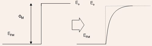
In the representation of the energy band diagram of the metal so far, an abrupt barrier of height
When the electron comes out of the metal, it faces an attractive force due to the positive image charge induced in the metal:
As a result of this force the potential energy varies as
The variation of potential energy with distance is illustrated by the Figure below:
In the presence of a constant electric field, the net potential energy can be written as:
The potential energy has a maxima resulting in lowering of barrier height by an amount
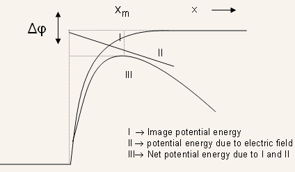 |
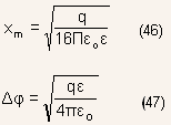
The analysis carried out for Metal-vacuum system can be extended to metal-semiconductor system as well with the difference that permittivity for Silicon should be used instead of that of vacuum.
Example 2.4 : Determine the barrier height of a Schottky diode at equilibrium using image force barrier lowering into account. Assume that
Solution : Taking
Use of Eq. (47) gives
As a result of barrier height lowering, the reverse current is not independent of voltage but increases significantly with increase in reverse bias.
As electric field increases further, avalanche multiplication begins to occur causing rapid increase in reverse current and eventually breakdown occurs. This is explained in more detail later on in the context of PN Junctions.
Example 2.5 : Sketch the energy band diagram for the metal semiconductor system shown below using simple work function theory and comment on whether the junction will have rectifying characteristics or not.

In this case the electrons will transfer from the metal into the N-type semiconductor and result in an accumulation of electrons at the surface. The final band diagram is shown below:
The barrier height