(i) Rectifying Schottky barrier diodes
(ii) Ohmic Contacts
- Schottky barrier diode is an important semiconductor device in
itself with applications including high speed rectifiers, Photodetectors,
etc
- Important part of other devices such as MESFETs, HEMTs etcMetal semiconductor Schottky barrier diodes are used as test structures for measuring doping, defect properties etc.
- Metal-semiconductor Ohmic contacts are an essential part of all semiconductor devices.
- We begin our discussions with an analysis of the junction in equilibrium.
As a first step,we will determine the energy band diagram of the junction.
- Semiconductor surface same as bulk
- No interfacial oxides etc
- Semiconductor: uniformly doped N-type Silicon
- Metal: Aluminum
- The energy band diagram of the junction is determined by first drawing the
band diagrams of metal and the semiconductor separately and then suitably
combining them.
Energy-band diagram before equilibrium 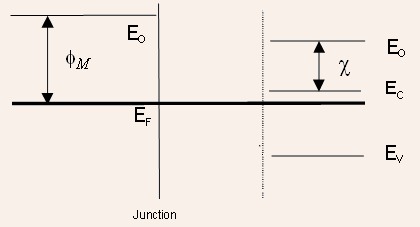
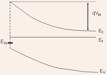
- After equilibrium, Fermi levels will align. This will be accompanied with transfer of electrons from semiconductor(higher Fermi level) to metal (lower Fermi level)
- Far from junction: band diagram of semiconductor same as before
 can
be easily drawn.
can
be easily drawn. - Metal unaffected by addition of small number of electrons: same
as before so that the following diagram can be easily sketched.
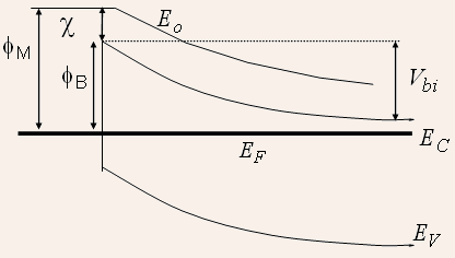
- As we approach the junction, the semiconductor gets progressively
depleted of electrons:
 bands
must bend upwards.
bands
must bend upwards.
| Energy-band diagram after equilibrium | |
|
|
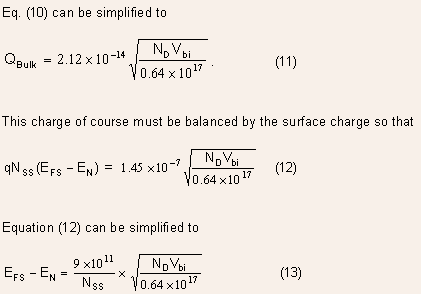
The barrier height can be expressed as:
Whenever two materials are brought into contact, a contact potential develops upon attainment of equilibrium. The contact potential is the difference in their work functions.
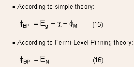
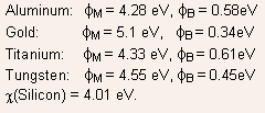
Example 1.1 Determine the contact potential for the following sets of metals deposited on N-type Silicon and compare it with experimentally measured values given below:
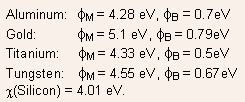
Solution : Using Eq.(1), we obtain the following set of values:
|
It can be seen from the table that the theoretically predicted barrier heights do not match well with the experimentally measured values at all. Despite change in workfunctions, the barrier heights do not change as much.
Wrong Assumption: Surface has characteristics same as the bulk semiconductor
Surface has a large number of energy levels within the bandgap unlike the bulk semiconductor. These energy levels are almost distributed in a continuous manner and are described by surface state density
Surface states either donor or acceptor-like, with each kind distributed within the bandgap.
Assumption: States above Fermi energy are unoccupied and those below it are occupied
The net charge at the surface can be expressed as :
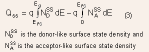
Eq. (3) shows that when
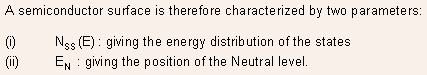
One can define now an energy level called neutral Level N E such that if Fermi energy at the surface were equal to it, the net charge at the surface would be zero.
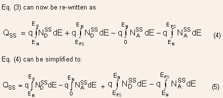
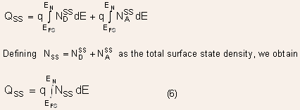
The first tem is zero by the definition of neutral level and the second term can be written as
If the Fermi energy at the surface(
Explanation: Compared to the case where
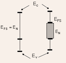 |
The consequences of a large surface state density is that Fermi energy at the surface is pinned to the neutral level irrespective of other factors such as doping in the bulk etc
Explanation: For simplicity, assume surface state density to be constant
This charge must be balanced by charge in the bulk
For an N-type semiconductor, positive depletion charge will balance the negative surface charge with energy band diagram as shown:
 |
Example 1.2 : For an N-type semiconductor of doping
Solution : This can be obtained using Eq.(13) provided Vbi is known. However, Vbi itself requires knowledge of
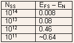 |
The results show that for
- Pinning of surface Fermi level at the neutral level implies:
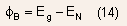
- The value given by Eq. (14) also does not agree all the time with experimental values if neutral level is assumed to remain at 0.33 eV
- A more sophisticated model i that takes into account presence of interfacial oxide(removal of second assumption) gives a better match with experimental results
- All the results derived for N-type Schottky barrier also apply to Schottky barriers on P-type semiconductors as well.
For N-type Si this is about 0.75 eV.
Example 1.3 : Determine the contact potential for the following sets of metals deposited on P-type Silicon using the ideal work function difference theory and compare it with experimentally measured values given below:
Solution : Using Eq.(15), we obtain the following set of values:
|
It can be seen that the workfunction theory does not explain the experimental results at all. According to the workfunction theory the sum of N-type Schottky barrier height and P-type Schottky barrier height should add up to the bandgap. This is roughly true for the experimentally measured values for Gold Titanium and Tungsten but not for Aluminum.
- Neither the simple work function difference theory nor the simple
Fermi level pinning theory adequately explains the experimental values.
A more complicated model that takes into account voltage drop across
interfacial oxide gives a better match.
- Almost all the metals form a junction with Silicon such that a barrier
exists for the flow of electrons in N-type material and for holes in
P-type material.
- A consequence of this is that semiconductor near the junction is depleted
of carriers and a space charge region exists.
- The detailed nature of potential variation, electric field, space
charge region’s width etc can be obtained through the solution
of Poisson Equation.
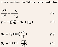
Assumptions:
(i) Neglect
(ii) All donors are ionized
(iii) Neglect
- The neglect of electron and hole density within the space charge region
is known as thedepletion approximation. The validity of this assumption
will be discussed in detail during the study of PN junctions.
Charge Profile after depletion approx.
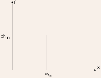
- With the depletion approximation, the Poisson equation can be easily
solved to obtain the following important results:
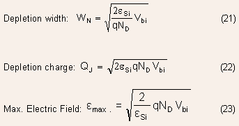
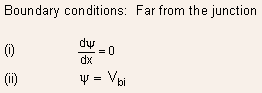
- Although derived for equilibrium, the equations remain valid for non zero values of applied voltage also, provided depletion approximation is assumed to hold. The only change that needs to be made is to substitute Vbi by Vbi - V , where V is the voltage applied between the metal and the semiconductor.
Example 1.4 : Determine the value of maximum electric field and depletion width for a Schottky barrier on N-type Silicon of doping
| Solution : | |
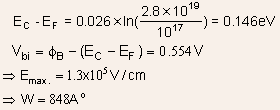 |