The current-voltage characteristics is of prime concern in the study
of semiconductor devices with light entering as a third variable in optoelectronics
devices.The external characteristics of the device is determined by the
interplay of the following internal variables:
The semiconductor equations relating these variables are given below:
Carrier density:
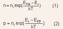
where is the electron quasi Fermi level and
  is
the hole quasi Fermi level. These two equations lead to
is
the hole quasi Fermi level. These two equations lead to
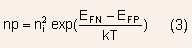
In equilibrium
= = Constant
Current:
There are two components of current; electron current density and
hole current density
and
hole current density  .
There are several mechanisms of current flow:
.
There are several mechanisms of current flow:
(i) Drift
(ii) Diffusion
(iii) thermionic emission
(iv) tunneling
The last two mechanisms are important often only at the interface of two different materials such as a metal-semiconductor junction or a semiconductor-semiconductor junction where the two semiconductors are of different materials. Tunneling is also important in the case of PN junctions where both sides are heavily doped.
In the bulk of semiconductor , the dominant conduction mechanisms involve drift and diffusion.
The current densities due to these two mechanisms can be written as
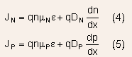
where are
electron and hole mobilities respectively and
are
electron and hole mobilities respectively and  are
their diffusion constants.
are
their diffusion constants.
Potential:
The potential and electric field within a semiconductor can be defined in the following ways:
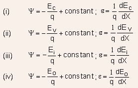
All these definitions are equivalent and one or the other may be chosen on the basis of convenience.The potential is related to the carrier densities by the Poisson equation: -
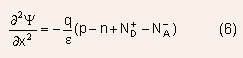
where the last two terms represent the ionized donor and acceptor density.
Continuity equations
These equations are basically particle conservation equations:
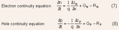
Where G and R represent carrier generation and recombination rates.Equations (1-8) will form the basis of most of the device analysis that shall be discussed later on. These equations require models for mobility and recombination along with models of contacts and boundaries.
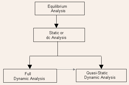
Analysis Flow
Like most subjects, the analysis of semiconductor devices is also carried out by starting from simpler problems and gradually progressing to more complex ones as described below:
(i) Analysis under zero excitation i.e. equilibrium.
(ii) Analysis under constant excitation: in other words dc or static characteristics.
(iii) Analysis under time varying excitation but with quasi-static approximation dynamic characteristics.
(iv) Analysis under time varying excitation: non quasi-static dynamic characteristics.
Even though there is zero external current and voltage in equilibrium, the situation inside the device is not so trivial. In general, voltages, charges and drift-diffusion current components at any given point within the semiconductor may not be zero.
Equilibrium in semiconductors implies the following:
(i) steady state:
Where Z is any physical quantity such as charge, voltage electric field etc
(ii) no net electrical current and thermal currents:
Since current can be carried by both electrons and holes, equilibrium implies zero values for both net electron current and net hole current. The drift and diffusion components of electron and hole currents need not be zero.
(iii) Constant Fermi energy:
The only equations that are relevant (others being zero!) for analysis in equilibrium are:
In equilibrium, there is only one independent variable out of the three variables :
If one of them is known, all the rest can be computed from the equations listed above. We shall take this independent variable to be potential.
The analysis problem in equilibrium is therefore determination of potential or equivalently, energy band diagram of the semiconductor device.
This is the reason why we begin discussions of all semiconductor devices with a sketch of its energy band diagram in equilibrium.
Energy Band Diagram
This diagram in qualitative form is sketched by following the following procedure:
Analysis in equilibrium: Solution of Poisson’s Equation with appropriate boundary conditions -
Non-equilibrium analysis:
There are two complementary ways of studying semiconductor devices:
(i) Through numerical simulation of the semiconductor equations.
(ii) Through analytical solution of semiconductor equations.
These techniques aim at arriving at closed form symbolic expressions linking important device characteristics. They have the following uses:
(i) They provide basic understanding of device operation
(ii) The devices models obtained are useful for use in circuit analysis
- Electron and hole currents
- Potential
- Electron and hole density
- Doping
- Temperature
The semiconductor equations relating these variables are given below:
Carrier density:
where
In equilibrium
Current:
There are two components of current; electron current density
(i) Drift
(ii) Diffusion
(iii) thermionic emission
(iv) tunneling
The last two mechanisms are important often only at the interface of two different materials such as a metal-semiconductor junction or a semiconductor-semiconductor junction where the two semiconductors are of different materials. Tunneling is also important in the case of PN junctions where both sides are heavily doped.
In the bulk of semiconductor , the dominant conduction mechanisms involve drift and diffusion.
The current densities due to these two mechanisms can be written as
where
Potential:
The potential and electric field within a semiconductor can be defined in the following ways:
All these definitions are equivalent and one or the other may be chosen on the basis of convenience.The potential is related to the carrier densities by the Poisson equation: -
where the last two terms represent the ionized donor and acceptor density.
Continuity equations
These equations are basically particle conservation equations:
Where G and R represent carrier generation and recombination rates.Equations (1-8) will form the basis of most of the device analysis that shall be discussed later on. These equations require models for mobility and recombination along with models of contacts and boundaries.
Analysis Flow
Like most subjects, the analysis of semiconductor devices is also carried out by starting from simpler problems and gradually progressing to more complex ones as described below:
(i) Analysis under zero excitation i.e. equilibrium.
(ii) Analysis under constant excitation: in other words dc or static characteristics.
(iii) Analysis under time varying excitation but with quasi-static approximation dynamic characteristics.
(iv) Analysis under time varying excitation: non quasi-static dynamic characteristics.
 |
Even though there is zero external current and voltage in equilibrium, the situation inside the device is not so trivial. In general, voltages, charges and drift-diffusion current components at any given point within the semiconductor may not be zero.
Equilibrium in semiconductors implies the following:
(i) steady state:
Where Z is any physical quantity such as charge, voltage electric field etc
(ii) no net electrical current and thermal currents:
Since current can be carried by both electrons and holes, equilibrium implies zero values for both net electron current and net hole current. The drift and diffusion components of electron and hole currents need not be zero.
(iii) Constant Fermi energy:
The only equations that are relevant (others being zero!) for analysis in equilibrium are:
| Poisson Eq: | 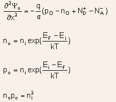 |
In equilibrium, there is only one independent variable out of the three variables :
If one of them is known, all the rest can be computed from the equations listed above. We shall take this independent variable to be potential.
The analysis problem in equilibrium is therefore determination of potential or equivalently, energy band diagram of the semiconductor device.
This is the reason why we begin discussions of all semiconductor devices with a sketch of its energy band diagram in equilibrium.
Energy Band Diagram
This diagram in qualitative form is sketched by following the following procedure:
- The semiconductor device is imagined to be formed by bringing together the various distinct semiconductor layers, metals or insulators of which it is composed. The starting point is therefore the energy band diagram of all the constituent layers.
- The band diagram of the composite device is sketched using the fact that after equilibrium, the Fermi energy is the same everywhere in the system. The equalization of the Fermi energy is accompanied with transfer of electrons from regions of higher Fermi energy to region of lower Fermi energy and viceversa for holes.
- The redistribution of charges results in electric field and creation of potential barriers in the system. These effects however are confined only close to the interface between the layers. The regions which are far from the interface remain as they were before the equilibrium
Analysis in equilibrium: Solution of Poisson’s Equation with appropriate boundary conditions -
Non-equilibrium analysis:
- The electron and hole densities are no longer related together by
the inverse relationship of Eq. (5) but through complex relationships
involving all three variables Y , , p
- The three variables are in general independent of each other in
the sense that a knowledge of two of them does not lead automatically
to a knowledge of the third.
- The concept of Fermi energy is no longer valid but new quantities
called the quasi-Fermi levels are used and these are not in general
constant.
- For static or dc analysis, the continuity equation becomes time
independent so that only ordinary differential equations need to be
solved.
- For dynamic analysis however, the partial differential equations have to be solved increasing the complexity of the analysis.
There are two complementary ways of studying semiconductor devices:
(i) Through numerical simulation of the semiconductor equations.
(ii) Through analytical solution of semiconductor equations.
- There are a variety of techniques used for device simulation with some of them starting from the drift diffusion formalism outlined earlier, while others take a more fundamental approach starting from the Boltzmann transport equation instead.
- In general, the numerical approach gives highly accurate results
but requires heavy computational effort also.
- The output of device simulation in the form of numerical values
for all internal variables requires relatively larger effort to understand
and extract important relationships among the device characteristics.
These techniques aim at arriving at closed form symbolic expressions linking important device characteristics. They have the following uses:
(i) They provide basic understanding of device operation
(ii) The devices models obtained are useful for use in circuit analysis
- Analytical solution of semiconductor equations under both equilibrium
and non-equilibrium conditions is often a difficult task and is carried
out using judicious use of assumptions to obtain simplification.
- For example, assumptions that electron or hole population in a
given region is in quasi-equilibrium is frequently used to simplify
the analysis.
- At other times, the quasi-static approximation is used to reduce
the problem of solving partial differential equation in dynamic analysis
to solution of ordinary differential equations only.
- Since, each assumption limits the range of validity of the obtained
results, the goal in analytical modeling is to use as few assumptions
as are necessary to obtain results which are general, accurate and
at the same time simple enough to comprehend and use for circuit analysis.
- It can rightfully be said that the art of analytical modeling is
the art of making assumptions!
- Since the requirements of generality, accuracy and simplicity are
often - mutually conflicting in nature, one or the other has to be
sacrificed.
- The first to be sacrificed is often generality. Instead of obtaining
a single model applicable over the entire range of excitation, a set
of models for different regions or modes of operation is derived.
In each region of operation, a different set of assumptions
is used to obtain a simple result.
- As expected, this sectioning of device operation into regions creates
problems at the boundaries by causing discontinuity in device characteristics.
|
||||||||||||||||||||||