In this chapter, design issues associated with analog and digital circuits
will be discussed in brief. To appreciate the design issues, some of
the important transistor parameters and their dependence on base and
collector doping and thicknesses are summarized below:
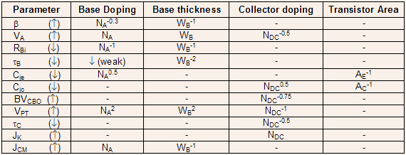
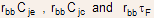
A number of important tradeoffs can be seen in the table shown above.
Tradeoffs:
- Eq. (1) shows that for a fixed base doping, an increase in current gain will be accompanied by an increase in base resistance as well. Similarly, Eq. (2) shows that for constant base doping, an increase in early voltage will result in decrease in current gain.
Example 7.1 Design an NPN transistor that has a current gain of 500 at
Solution : What will be described here is a first pass at design.
Various assumptions that are made will have to refined in the next iteration.
![]()
We take ![]() The corresponding bandgap narrowing in emitter is
The corresponding bandgap narrowing in emitter is ![]() ,
,
We take ![]()
We will take small doping in the base so as to obtain this high value of gain. As a result BGN in base can be neglected.
This gives ![]() .
We have several choices here for base doping and the resulting base
thickness. Let us take
.
We have several choices here for base doping and the resulting base
thickness. Let us take ![]()
This is the effective base width. Let us calculate the metallurgical base width. For this we will have to calculate the depletion regions within the base due to emitter-base and collector-base junctions.
For the emitter base junction we assume a forward bias of 0.7 volts and built-in voltage of 0.95 Volts. Most of the depletion region will lie in the base so that
![]()
Similarly, the depletion width due to collector junction can be calculated:
![]()
The metallurgical base width will be ![]()
The punchthrough voltage for such a lightly doped and narrow-base can be calculated using the expression
![]()
This is a very small voltage meaning that transistor can only be operated close to zero collector-base voltage. The early voltage of the transistor is also very small.Thus a large current gain is obtained only at the expense of very small punchthrough and Early voltages. The base resistance is also very large.
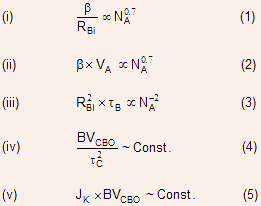
- Eq. (1-3) also show that overall transistor characteristics can
be improved by increasing the doping level in the base. The base thickness
has to be simultaneously scaled to maintain a constant current gain
and to improve the base transit time.
- The transistor area should be scaled so as to reduce the emitter and collector junction capacitances.
A general guideline for improving the performance of a BJT would therefore be:
- increase base doping
- reduce base thickness
- reduce device area
- minimize the extrinsic transistor region
These tasks have to be done such that:
- punchthrough does not occur in the base
- high-level injection does not occur in the base
- high-level injection does not occur in the collector
- collector-base breakdown voltage is adequate
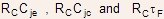
In order to appreciate the design issues in more detail, let us first look at the demands imposed on the transistor by some common analog circuit blocks. The Figure below shows a common emitter amplifier(without the biasing network):
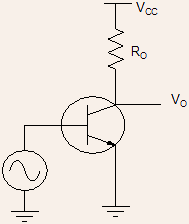
The important characteristics of a common emitter include :
-
Since a high voltage gain , a high input resistance and a low output resistance are the desirable characteristics of a CE amplifier, we would like to have a transistor with as high a current gain as possible.
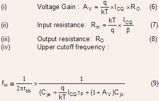
- To improve the upper cutoff frequency, the terms;
 .
.
Since :
![]()
Where ![]() its width (perpendicular to the plane of the paper)
its width (perpendicular to the plane of the paper)
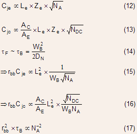
- Eq. (15-17) show that frequency performance can be improved by reducing
emitter length Le , increasing base doping NA and reducing collector
doping NDC. The base thickness has to be reduced even though it tends
to increase the time constants described by Eq. (15-16), so as to
maintain a constant current gain.
- Eq. (16) shows that the collector-base junction area should be made
close to the base –emitter junction area by reducing the extrinsic
transistor region.
- Since collector current is dictated by the circuit, the scaling
of device dimensions to improve the frequency performance will be
accompanied by an increase in collector current density. Therefore,
steps should be taken so as to avoid onset of high level
injection effects at the operating current density.
- The actual design of base and collector regions would depend on
the relative importance of different time constants in the expression
of upper cutoff frequency.
- For example, if the amplifier is biased at low collector currents
and voltage gain is small, then the time constant described by Eq.
(15) may be the most important. If we remember that:
then using Eq. (18) and Eq. (15)
- In other words, increase in base doping will have little impact on the frequency performance. The best way of improving the performance will be via scaling of emitter length.
- Let us consider another situation where the amplifier is biased
at large collector current so that the time constant described by
Eq. (17) is the most important. For this case,
- In this case, scaling will not have any impact but increase in base doping and scaling of base width will considerably improve the circuit performance.
- What this example shows is that different transistor characteristic
and therefore different designs are required for different circuit
applications. In discrete circuits, this can be handled by using different
kinds of transistors for different circuits but for
monolithic circuits, the same transistor has to be used in all the circuits thereby complicating the transistor design. - The importance of high base doping stems largely from the reduction
in base resistance that it leads to. Suppose the amplifier shown in
the earlier Figure is driven by a resistance RC which is considerably
larger than the base resistance as shown below:
- To improve the upper cutoff frequency now, the terms;
 have to be minimized. From the transistor’s point of view, this
means that the capacitances and the base transit time should be minimum.
As earlier, for low collector currents and small voltage gain, the
term involving emitter junction capacitance will be the most important
term. Since,
have to be minimized. From the transistor’s point of view, this
means that the capacitances and the base transit time should be minimum.
As earlier, for low collector currents and small voltage gain, the
term involving emitter junction capacitance will be the most important
term. Since, ,
a base with low doping level will be better !
,
a base with low doping level will be better !
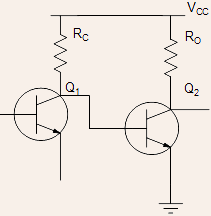
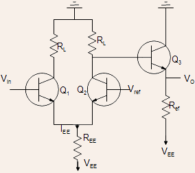
Let us consider another circuit which is commonly used in analog circuits: an amplifier with an active load:
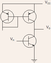
- The voltage gain for the CE amplifier with an active load can be
written as:
As before,
The upper cutoff frequency may be dominated by the collector junction capacitance due to very high voltage gain
As a result, the collector junction capacitance acquires the highest importance. Eq. (16) along with the expression for current gain give:
A high doping in the base and low doping in the collector are the requirements now. The base thickness needs to be only slightly scaled so as to maintain a constant current gain.
Example 7.2 Figure below shows an CE amplifier with an active load. Design a transistor for such a circuit such that it has
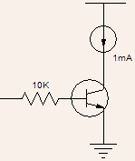
Solution : As in the previous example, We take
The corresponding bandgap narrowing in emitter is
We take
We will take small doping in the base so as to obtain the given value of gain. As a result BGN in base can be neglected.
This gives
Suppose we take
This gives
So far we have calculated the early voltage at zero collector-base bias. If the voltage is calculated for
where
The current handling capability should be better than 1mA so that
Since Area =
Final design:
Only the effective base width is given above. With all the doping values available, the corresponding metallurgical base width can be easily determined.
In the front amplifier stages, the voltages are low and breakdown is not as important as in the output stages where voltage swings are larger.
Let us next consider the design issues associated with a BJT in a digital circuit. For this we shall take an ECL gate as an example:
For the 10K series gate these values=4mA and total power dissipation
Among the important characteristics of an ECL gate are:
- propagation delay
- power dissipation
- noise margin
- Area
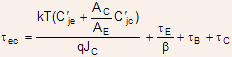
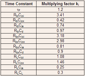
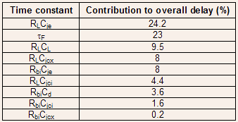
The propagation delay is a complicated function of various capacitances and resistance in the transistor. It can be modeled as:
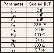
The various time constant and the multiplying factors are listed below:
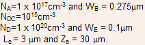
Example 7.3 Consider an ECL circuit fabricated using a 6
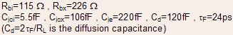
The ECL circuit had
Solution : The gate delay turns out to be ~316ps. The contributions of some of the important time constants is given below:
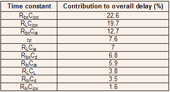
The emitter junction capacitance accounts for about 25.6% of the delay and is the next important capacitance.
The forward transit time, which is basically, the base transit time accounts for about 14.4% of the overall delay.
As a result, the approach for reducing the overall delay would be to :
- reduce the extrinsic collector-base area to reduce the extrinsic
collector junction capacitance
- reduce the extrinsic base resistance
- scale the area to reduce both the collector as well as emitter junction
capacitances
- scale the base width to reduce the base transit time
The transistor described above was a non-self-aligned structure typical
of transistors used in ![]()
- Through use of self-aligned techniques, both the extrinsic base
resistance, as well as extrinsic base capacitance can be sharply reduced
resulting in overall improvement in delay.
These self aligned structures are described below:
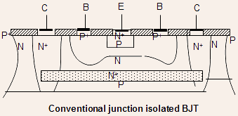
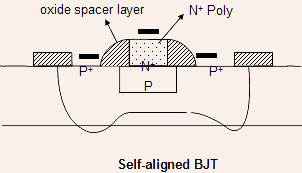
- The oxide spacer layer shown in the self aligned structure is very
narrow so that the base contact is very close to the intrinsic base
region as compared to the non self aligned structure shown in the
first Figure. The use of
 poly
silicon facilitates formation of the spacer to isolate emitter and
base contacts and also improves the current gain.
poly
silicon facilitates formation of the spacer to isolate emitter and
base contacts and also improves the current gain.
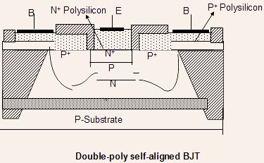
Note that the base contact is formed on the Poly which makes the contact with the extrinsic base region.
- As mentioned earlier, use of self aligned techniques will improve
the transistor characteristics and ECL propagation delay through reduction
in extrinsic base and collector resistances.
Example 7.4 Calculate the ECL gate delay and determine the relative contributions of different factors for a self aligned transistor described below Also shown for comparison are the characteristics of a non self-aligned transistor.
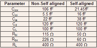
Both the transistors have dimensions of 6mm x 6mm and are quite similar to each other except for the fact that base is self aligned to the emitter in the second case.
Solution : The overall ECL delay reduces to 157ps. The relative importance of different time constants becomes different now!
Examination of the table shows that emitter junction capacitance is the most important one accounting for almost 32% of the overall delay. The extrinsic collector capacitance accounts for only 8% of the delay.
- The base transit time now represents 27% of the delay.
- The most important resistance is the load resistance of the ECL
gate accounting for almost 46% of the delay.
- The next important resistance is the intrinsic base resistance accounting
for about 13.4% of the overall delay.
The ECL delay can now be improved through the following techniques:
On the circuit side, reduction in load resistance will pay rich dividends but it would increase the supply current according to the expression.
where
- The other way of avoiding an increase in current is by scaling
the voltage swing along with scaling of load resistance. This would
result in decrease of noise margin. Nevertheless, voltage swing
has been reduced in ECL circuits over the years.
- An increase in supply current may not result in increased power
dissipation if the supply voltage is scaled. This trend can also
be seen over the years.
- Even if current is maintained constant, due to scaling of device
size, the collector current density inside the BJT will increase
so that steps to avoid high level injection in base and collector
have to be taken during the design.
The table below shows the relative contributions of different time constants for an ECL circuit fabricated using a selfaligned transistor of dimensions
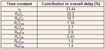
The overall delay is ~20ps
- The base transit time is the most important factor now. It accounts
for nearly 47% of the delay.
- The emitter junction capacitance now accounts for less than 4%
of the delay as a result of scaling.
- The extrinsic collector junction now accounts for about 7% of
the delay and is the most importance capacitance now after the diffusion
capacitance represented by base transit time. The renewed importance
of extrinsic collector-base capacitance is because the extrinsic
region does not scale as fast as the intrinsic region.
- The other important capacitance is the load capacitance. Its contribution to delay has jumped from 9.5% to 22.2%.
- The most important resistance is the load resistance again accounting for about 34.5% of the delay. Next to it is the intrinsic base resistance accounting for nearly 14% of the delay.
- The trend seen so far indicates that with continued improvement
in BJT characteristics, the eventual ECL delay would be decided
by the
 term!
term!
These results suggest that delay can be further reduced by:
- scaling the base thickness to reduce base transit time
- increasing the base doping to reduce the intrinsic base resistance and avoid punchthrough and high level injection in the base.
The collector current density for the above example is ~4x10 4 A/cm 2 !. The current density for onset of high level injection in collector is ~7x10 4 A/cm 2 for a collector doping of
- The scaling of transistor area may not yield much improvement
in delay because of the small contributions of area dependent junction
capacitances. However, as base doping is raised along with scaling
of base thickness, the emitter junction capacitance will increase
which can be kept in check through suitable scaling of transistor
area.
- As a result major improvement in transistor performance will
now come as a result of reduction in forward transit time through
scaling of base width and simultaneously increasing the base doping
to avoid punchthrough, high level injection and reducing the base
resistance. The collector doping will also have to be raised to
avoid high level injection in the collector and to reduce the collector
transit time which becomes increasingly more important as base transit
time is continually reduced.
- As the base doping is increased, the emitter-base junction tends
to become of
 type. This junction begins to have a very low breakdown voltage
and high leakage currents associated with tunneling. As a result
of this, the base doping is limited less than about
type. This junction begins to have a very low breakdown voltage
and high leakage currents associated with tunneling. As a result
of this, the base doping is limited less than about  .
.
- This has very serious consequences. If base doping cannot be
increased beyond a limit, then base thickness can also not be scaled
beyond a limit otherwise punchthrough would occur. The base resistance
would also become constant due to limitation on base doping.
- This means that transistor’s performance cannot be improved
beyond a certain point.
Example 7.5 Suppose the base doping is limited to ![]() What
is the minimum base width we can have such the transistor can handle
a reverse collector voltage of 5 volts?
What
is the minimum base width we can have such the transistor can handle
a reverse collector voltage of 5 volts?
(b) Will this value of base width be useful for transistor operation?
Solution : Using the expression for punchthrough voltage:
![]()
We obtain ![]()
(b) Such a small base width will first of all be difficult to fabricate.
But besides that let us look at other consequences. The depletion
region due to emitter junction calculated to be 98.5 ![]() and
that due to collector junction for a collector doping of
and
that due to collector junction for a collector doping of ![]() Thus
the effective base width will be
Thus
the effective base width will be ![]() This
would yield a base transit time of only 0.156 ps which is good but
really not necessary when for example the collector transit time for
This
would yield a base transit time of only 0.156 ps which is good but
really not necessary when for example the collector transit time for
![]() is
itself 1.6ps. The current gain for an emitter doping of
is
itself 1.6ps. The current gain for an emitter doping of ![]() and thickness of 0.1
and thickness of 0.1![]() can
be evaluated to be 590 which is also good.
can
be evaluated to be 590 which is also good.
However, the early voltage is only 16 Volts at zero collector-base
bias. Further the sheet resistance of the base can be calculated to
be :
![]() .
.
For a minimum geometry transistor where ![]() the
base resistance will be
the
base resistance will be ![]() ,
which is very large.
,
which is very large.
- The source of this limitation is stemming from the emitter base
junction becoming heavily doped junction on both sides. This can
be avoided by making the emitter lightly doped to say a doping of
around
 The
base doping can be increased now without increasing the tunneling
leakage currents. The base thickness can also be scaled now. But
a lowly doped emitter and heavily doped base will have a current
gain less than unity !. Such a device would be useless for all applications.
The
base doping can be increased now without increasing the tunneling
leakage currents. The base thickness can also be scaled now. But
a lowly doped emitter and heavily doped base will have a current
gain less than unity !. Such a device would be useless for all applications.
- The expression for current gain shows that there is a way of
making a transistor with lightly doped emitter and heavily doped
base and still get a high current gain:
Normally due to heavy doping in the emitter as compared to the collector, the bandgap in emitter is smaller than that in the base so that the first term is much less than unity.
- However, if we now make the emitter using a material which has
a larger bandgap as compared to the material used in the base then
a very high current gain can be obtained despite a low emitter doping
and a high base doping level.
For example, if the difference in the bandgaps of emitter and base is 0.4eV, then for emitter doping of and
base doping of
and
base doping of  the
current gain for comparable emitter and base thicknesses turns out
to be
the
current gain for comparable emitter and base thicknesses turns out
to be
- A BJT which is fabricated using different semiconductors in emitter
and base is known as a heterojunction bipolar transistor or simply

In an HBT the base doping can be made very high and base thickness very small so that very low intrinsic base resistance and base transit times can be obtained.
Example 7.6 Suppose the base is heavily doped to the tune
of ![]() and
emitter lightly doped but current gain is maintained at a reasonable
value through use of wide bandgap semiconductor emitter. What will
be the resulting changes in Transistor’s characteristics as compared
to the previous example?
and
emitter lightly doped but current gain is maintained at a reasonable
value through use of wide bandgap semiconductor emitter. What will
be the resulting changes in Transistor’s characteristics as compared
to the previous example?
Solution : For a similar effective base thickness of ![]() and
for the moment ignoring the reduction in mobility as a result of increased
base doping, the base resistance will reduce to 260
and
for the moment ignoring the reduction in mobility as a result of increased
base doping, the base resistance will reduce to 260 ![]() and
Early voltage will increase to 800 !. The unity gain frequency will
be determined by collector transit time because the base transit time
is so small.
and
Early voltage will increase to 800 !. The unity gain frequency will
be determined by collector transit time because the base transit time
is so small.