- There are two high-level injection effects that we
shall discuss here:
(i) High Level injection in Base
(ii) High level injection in Collector
We shall consider high level injection in the base, also termed as Webster effecti,
first:
effecti,
first:
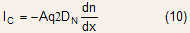
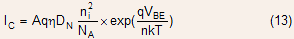
For simplicity, we shall consider a uniformly doped base. The expression for collector current that has been used in the past discussion was based on low level injection approximation. This approximation allowed the collector current to be expressed as a purely electron diffusion current:
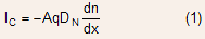
Neglect of recombination results in linear variation of electron density across the base so that
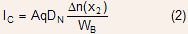
The second simplification that low level injection resulted in was that the expression:
With these three simplifications, the collector current can be written as:
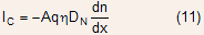
When the injected electron density begins to become comparable to the base doping, the electron current begins to have an appreciable drift component as well. Assuming that the hole current in the base and therefore the base current is small, we can obtain the magnitude of the electric field in the base:.
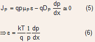
With this expression, the collector current can be expressed as sum of drift and diffusion terms:
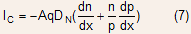
The base is quasi-neutral and uniformly doped as that:
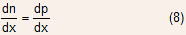
This allows Eq. (7) to be written as
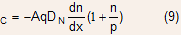
Eq. (9) shows that when injected electron density is much smaller, than the hole density in the base, the current is same as before and diffusive.
At very high current densities, so that
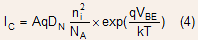
In general, the collector current can be expressed as
where
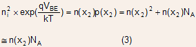
Under high-level injection conditions, the approximation made in Eq. (3) is no longer valid so that a full expression for electron density has to be used:
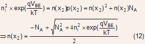
The electron density and therefore the collector current no longer increase as but
as
but
as 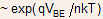 ,where
the ideality factor is unity for small base-emitter voltages but tends
to approach 2 at high biases.
,where
the ideality factor is unity for small base-emitter voltages but tends
to approach 2 at high biases.
The collector current under high level injection can therefore be modeled as
- The major impact of high level injection is that the
ideality factor of the collector current departs from unity and approaches
a value of 2.
- The base current, being due to injection of holes into
the emitter, continues to have an ideality factor of unity because low
level injection conditions continue to prevail in emitter due to its
heavy doping level.
- The increase in ideality factor of collector current
and a constant ideality factor of unity for base current means that
the collector current does not increase as rapidly as the base current
with increase in bias. As a result current gain will decrease!
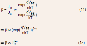
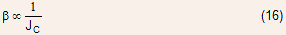
Eq. (15) shows that current gain will decrease with increase in collector current density. For very high collector current densities:
- This rapid decrease in current with increase in collector
current density means that the device quickly becomes useless since
almost all applications require at least a moderate value of current
gain.
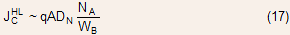
- As a measure of the collector current density at which high level
injection effects begin to become appreciable, we take
 so
that
so
that
- When the injected electron density becomes comparable
to the background doping in the base, it begins to affect the collector-base
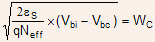
depletion region on the base side also. The charge density given by:

would increase because electron density adds to the charge due to acceptor atoms. This increase in charge density would result in decrease in depletion width on the base side thereby increasing the effective base width.
- This base pushout effect, besides decreasing collector
current and therefore the current gain, will also tend to increase the
base transit time.
- There is a counteracting effect due to the presence
of electric field in the base but in general the onset of high level
injection results in degradation of unity gain frequency.
Conductivity Modulation
The high-level injection phenomenon is also called conductivity modulation. The conductivity of base can be expressed as
Eq. (21) shows that as the injected electron density begins to become comparable to the base doping, the base conductivity will begin to increase with increase in collector density.
-
Example 4.1 (a)For an NPN transistor whose description is given below, determine the collector current after which the current gain will begin to fall.

(b)Discuss how can you double the value of maximum collector current.
Solution : The collector current density and collector current can be found using Eq. (17) to be and
3.62 mA respectively.
and
3.62 mA respectively.
(b) An obvious way of doubling the collector current would be to double the transistor area. Besides occupying more area on Silicon wafer, this approach would also double all the junction capacitances thereby adversely affecting the frequency response of the device. Another approach could be by doubling the base doping. This would however decrease the current gain also. A third method could be by reducing the base thickness. This would decrease the Early voltage and as we shall see in the next section also lower what is called the punchthrough voltage of the transistor.
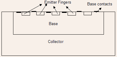
Current Crowding
The Figure below shows a simplified schematic of a Bipolar Transistor :
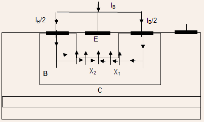
The structure has two base contacts, one on each side of the emitter. As a result of the lateral resistance of intrinsic base region
( ),
there will be a voltage drop across it.
),
there will be a voltage drop across it.
This means that the potential at the edge of the emitter (point )
will be larger than the potential in the middle (point
)
will be larger than the potential in the middle (point  ). Since the
emitter voltage is the same everywhere,

This means that a larger fraction of collector current would flow at the edges than at the center.
-
This phenomenon will increase as the current increases so that at very high currents, the entire collector current may flow only at the edges. This is known as current crowding. There are several adverse effects of current crowding at the emitter including
(i) Since all the current is confined at the emitter periphery, all the power will also be dissipated in a very narrow region resulting in localized heating which may damage the transistor
(ii) Since the current flows in a very narrow area close to the emitter edge, the collector current density will become very high resulting in early onset of high-level injection effects.
The onset of current crowding effect may be taken as the base current at which the lateral voltage drop becomes comparable to the thermal voltage :
:
The lateral base resistance can be expressed as
where are
emitter length and width respectively.
are
emitter length and width respectively.
Using Eq. (25) and (24) , the collector current density for the onset of current crowding can be expressed as:
Eq. (26) shows that current crowding decreases as the emitter length is reduced. It is for this reason that high power bipolar transistors are fabricated using a finger like structure with multiple emitter regions sandwiched between base contact regions as shown in the Figure below:
-
Eq. (26) also seems to suggest that an increase in base doping and thickness will also reduce current crowding due to decrease in base resistance. However, an increase in base doping or thickness will also reduce the current gain. If the expression for current gain derived earlier is taken, then it can be shown that
.gif) is independent of base thickness and increases as
is independent of base thickness and increases as  .
.
Example 4.2 For an NPN transistor whose description is given below, determine
(a) the maximum collector current limited by current crowding considerations
(b) Discuss different ways by which the maximum collector current can be increased by a factor of 9.

Solution :
(b)To increase collector current by a factor of 9, let us increase the transistor area by same factor to 15µm x 15µm. However, now
= 9.55 x 
 so
that maximum collector current remains
so
that maximum collector current remains .gif) = 2.16 mA. So a simple scaling up of transistor area will not work.
Suppose we decrease the emitter length while keeping the transistor
area the same so that now the transistor has a rectangular (1.66µm
x 15µm) rather than square geometry. Now the current crowding
limited current density increases to
= 7.74 x
= 2.16 mA. So a simple scaling up of transistor area will not work.
Suppose we decrease the emitter length while keeping the transistor
area the same so that now the transistor has a rectangular (1.66µm
x 15µm) rather than square geometry. Now the current crowding
limited current density increases to
= 7.74 x  and
=
19.44 mA, which is the desired value. However, this approach requires
advanced lithography to obtain a dimension of 1.6µm, which may
pose problems. A third approach could be to use 9 emitter fingers,
each of dimension 5µm x 5µm in a manner shown in the Figure
on the previous page. Now
remains same at 8.6 x
and
=
19.44 mA, which is the desired value. However, this approach requires
advanced lithography to obtain a dimension of 1.6µm, which may
pose problems. A third approach could be to use 9 emitter fingers,
each of dimension 5µm x 5µm in a manner shown in the Figure
on the previous page. Now
remains same at 8.6 x  but
total collector current increases nine times. There are other ways
of increasing the collector current by increasing base doping etc
but each comes at a price.
but
total collector current increases nine times. There are other ways
of increasing the collector current by increasing base doping etc
but each comes at a price.
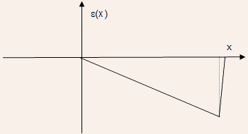
High Level Injection in Collector
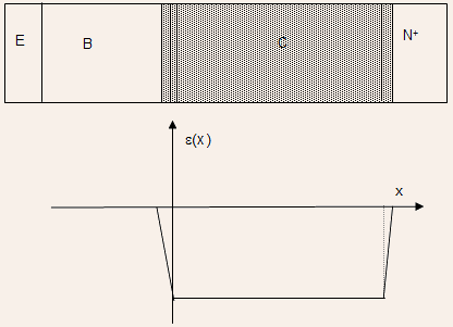
We shall assume for the most part that collector doping is considerably smaller than the base doping. As a result, the collector depletion region would lie mostly on the collector side as illustrated by the electric field profile shown below:
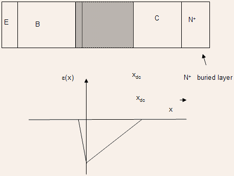
The effective doping in the collector is less than the background doping due to the storage of electrons in the depletion region required for flow of collector current.

-
As the collector current density increases, the effective collector doping decreases resulting in an increase of collector depletion width. This would result in increase of collector transit time
 and
a decrease in unity gain frequency.
and
a decrease in unity gain frequency.
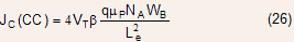
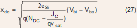
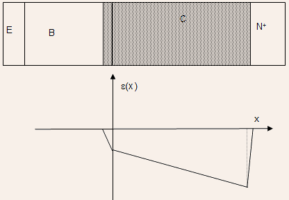
Eq. (27) predicts an infinite depletion width for a collector current density of

However, the depletion width does not become infinite but simply touches the buried
layer. The effective collector doping being zero for this case, the
collector can be though of as intrinsic layer. The electric field
profile for this case will be
buried
layer. The effective collector doping being zero for this case, the
collector can be though of as intrinsic layer. The electric field
profile for this case will be
-
The collector-base junction is like a PIN junction now!
-
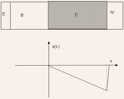
With further increase in collector current density, the effective collector doping becomes negative, implying a P-like semiconductor layer. The junction now shifts to the buried layer as illustrated by the Figure below:
With continued increase in collector current density, the depletion region withdraws from the base completely as illustrated by the next Figure.
·With even further increase in collector current density, the effective P-like doping increases further so that the space charge region begins to withdraw even from the collector region leaving behind a quasi-neutral collector region called a current induced
base!
This is illustrated in the next Figure.
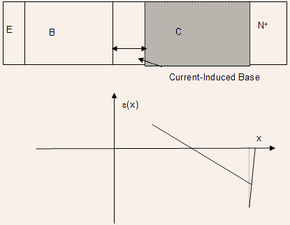
The formation of current-induced base further degrades the base transit time and unity gain frequency!
The onset of high level injection or the Kirk effect can be taken as the collector current density given by Eq. (28). At this collector current density, the collector becomes like an intrinsic layer!
Example 4.3 For an NPN transistor whose description is given below, determine the collector current after which the high level injection will begin to occur in the collector:
 and thickness 0.5µm followed by a thick heavily doped N-layer.
(b) At what current will the current induced base begin to form.
Solution : The Kirk current density is given by The collector current can then be calculated to be 3.2 mA
(b) When the current induced is about to form, the collector junction has shifted to theregion
and the N-region is like a P-type region as shown below
The effective P-type doping of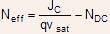 The
total depletion width, when current induced just begins to form now
is
The
total depletion width, when current induced just begins to form now
is so
that
so
that
This gives which then gives a collector current density of 5.5 x This
translates into a collector current of 5.5 mA.
which then gives a collector current density of 5.5 x This
translates into a collector current of 5.5 mA.