The emitter-base junction is forward biased and collector-base junction is reverse biased.Ignoring the reverse saturation current of the collector-base diode, the transistor can be represented as:
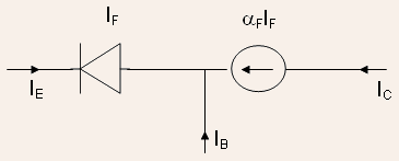
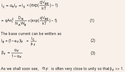
A small change in the base current would appear in an amplified form
at the collector current. In other words, the BJT exhibits current gain
and ![]() is
called its forward current gain.
is
called its forward current gain.
(Henceforth the subscript F will be dropped. Unless otherwise stated,
the mode of operation by default is the forward active mode).
Let us look at current gain in more detail:
The base current supplies the holes needed to replenish those that are
lost from the base
due to injection/recombination. It has four distinct components :
(i) ![]() this
supplies the holes lost due to recombination in the neutral base region
.
this
supplies the holes lost due to recombination in the neutral base region
.
(ii) ![]() this
supplies the holes that are injected into the emitter.
this
supplies the holes that are injected into the emitter.
(iii) ![]() this
supplies the holes that recombine within the EB space charge region.
this
supplies the holes that recombine within the EB space charge region.
(iv) ![]() this
represents the holes that flow from the CB space charge region into the
base as part of the reverse generation current.
this
represents the holes that flow from the CB space charge region into the
base as part of the reverse generation current.
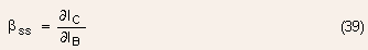
The current gain can therefore be written as:
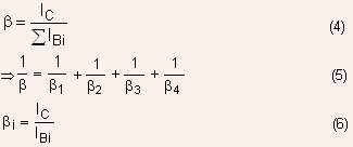
Eq. (5) shows that the component of current gain, which is the least, will determine the overall current gain. Let us try to estimate each one of the current gain components:
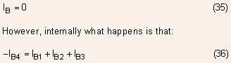
(i) The base current due to recombination within the neutral portion of the base can be written as
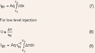
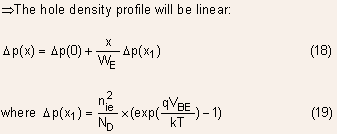
This requires determination of electron density within the base. It was shown earlier that if base recombination is neglected, then electron density varies linearly as shown below:
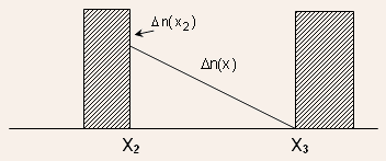
- It may seem strange that we are trying to estimate recombination within the base and using neglect of recombination within the base to find the electron density!
- However, it must be remembered that an assumption is good or bad depending on the context.
- It turns out that the profile of electron density in the base with recombination taken into account differs very slightly from the case where it is assumed to be linear, so we are justified in using this assumption.
![]()
The base current due to recombination within the base can then be expressed
as :
- Current gain is proportional to the recombination lifetime in the
base and inversely proportional to the base width. The current gain
is also independent of collector current.
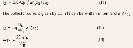
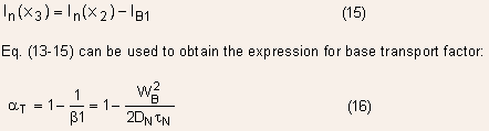
There is a parameter called the base transport factor, which is closely
related to the component of current gain just calculated. The base transport
factor is defined as the fraction of electron current, injected by the
emitter, that reaches the collector: 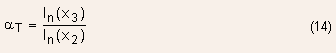
The fraction of electrons that do not reach the collector junction are
those that get lost due to recombination so that
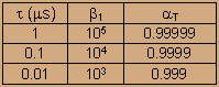
Example 2.1 : Determine the current gain component due to neutral base recombination for base recombination lifetimes of 1, 0.1 and 0.01 ms. Calculate also the base transport factor .
Solution : The calculated values are shown below :
Example 2.2 : Repeat the calculations for a base width of 5 mm.
Solution: The calculated values are shown below :
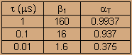 |
These two examples show that for a narrow base transistor suitable for high frequency digital and analog circuit applications, the neutral base recombination does not play a role and as result the base recombination lifetime is relatively unimportant. However, transistors designed for power applications have a large base width where neutral base recombination plays an important role and thus it is crucial to obtain high recombination lifetime.
| Current Gain Component due to injection of holes into the emitter |
For a uniformly doped emitter, the hole current can be assumed to be a diffusion current because low-level injection condition is always valid in emitter due to its heavy doping level:
![]()
The emitter region is as thin or even thinner than the base so that despite a lower recombination lifetime, the number of holes lost due to recombination within the emitter can be assumed to be negligible.
![]() is the intrinsic
carrier concentration in the emitter. The intrinsic carrier concentration
depends on the band gap:
is the intrinsic
carrier concentration in the emitter. The intrinsic carrier concentration
depends on the band gap:
![]()
| Heavy Doping Effects |
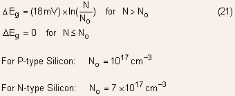
For small and moderate doping levels, the bandgap is independent of doping. But at higher doping levels, the bandgap decreases with increase in doping level i . Due to different doping levels in the base and emitter, the bandgap and therefore the intrinsiccarrier concentrations will also be different.
![]() There
are a variety of empirical models for this bandgap narrowing effect, the
simplest of which is:
There
are a variety of empirical models for this bandgap narrowing effect, the
simplest of which is:
![]() The
base current due to hole injection into the emitter can then be expressed
as:
The
base current due to hole injection into the emitter can then be expressed
as:
![]()
Using Eq. (12) and Eq. (22) and the expressions for ![]() ,
derived earlier, the current gain can be expressed as:
,
derived earlier, the current gain can be expressed as:
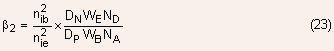
Use of bandgap narrowing model described by Eq. (21) allows the above equation to be simplified to :
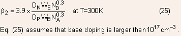
Example 2.3 : Determine the current gain component due to hole injection into the emitter without taking band gap narrowing into account, for the following set of values:
Solution : The current gain without bandgap narrowing will be:
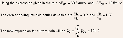
Example 2.4 : Calculate the bandgap narrowing in emitter and base and the resulting changes in intrinsic carrier concentrations. Re-calculate the current gain.
Example 2.5 : In the example above, suppose the emitter doping is increased to
Solution : For the new emitter doping
Emitter Injection efficiency
A parameter which is closely related to the current gain component
The emitter injection efficiency is a measure of how efficient the emitter is in injecting electrons into the base. It is important because the entire transistor action is due to the electrons injected into the base. The holes, which are simultaneously injected into the emitter, are useless from this point of view.
Eq. (27) can be re-written as :
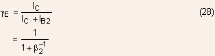
Using the expression for ![]() derived
earlier, the emitter injection efficiency can be written as,
derived
earlier, the emitter injection efficiency can be written as,

As noted earlier, the overall current gain is determined primarily by the base current resulting from injection of holes into the emitter. As a result, the current gain can be expressed in terms of emitter injection efficiency :
![]()
A high emitter injection efficiency is therefore necessary to obtain a high current gain.
The component of base current due to recombination within the emitter-base
space charge region can be expressed using Eq. (89) in the chapter on
PN junctions as:
![]()
It is assumed here that the space charge region lies entirely on the base
side because the base doping is much smaller than the emitter doping.
Using the expression for collector current given by Eq. (1), we obtain
:
This component of current gain is sensitive to recombination lifetime and varies with collector current density.
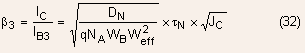
Example 2.6: Determine the current gain component due to SCR recombination
for current densities of ![]()
Take ![]() ,
base doping of
,
base doping of ![]() ,
effective base thickness of
,
effective base thickness of ![]() and
effective width of SCR recombination
and
effective width of SCR recombination ![]()
Solution : Using Eq. (32) we obtain
![]()
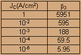 |
The table above shows that for current densities larger than
The last component of base current
![]()
- A quick calculation shows that this base current component is much smaller than the rest and can be ignored.
- There are however, situations where this current becomes the most
important base current component. For example, there are devices called
phototransistors, which are
basically BJTs whose excitation is optical instead of electrical.
As a result of optical excitation, electron-hole pairs are generated,
mostly in the collector-base depletion region. The phototransistor is
operated with its base floating so that
The optically excited holes supply the rest of the base current components
so that they are non-zero. As we noted earlier, the second component will
be the largest so that
![]()
The optically excited current gets multiplied by the current gain and
appears in an amplified form at the collector.
| Overall current Gain |
Taking all the components of the base current into account, we can draw the following conclusions:
- at very low collector current densities, the current gain is determined
primarily by recombination within the emitter-base space charge region.
In this regime the current gain increases with the collector-current
density and is sensitive to the recombination lifetime in the base.
- At higher collector current densities, the current gain is determined
primarily by injection of holes into the emitter or in other words emitter
injection efficiency.
- The current gain limited by emitter injection efficiency is independent of collector current as long as low level injection condition prevails in the base. As we shall see later, at very high collector current densities, the current gain begins to decrease.
The variation of current gain with collector current density can be represented
by the following Figure:
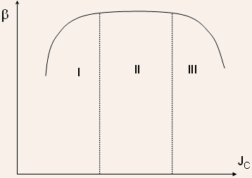
| I - Low current density II - Medium current density III - High current density |
Example 2.7 (a) By using the values calculated in earlier examples, determine the overall current gain at a collector current density of
(b) At what collector current density, does the current gain fall below unity?
(c) If recombination lifetime reduces to ![]() determine
the collector current density beyond which the current gain will be practically
constant.
determine
the collector current density beyond which the current gain will be practically
constant.
Solution : (a) The different current gain components are![]()
![]() so
that the current gain is primarily determined by emitter injection efficiency
.
so
that the current gain is primarily determined by emitter injection efficiency
.
( b) This requires that the SCR limited current gain reduce almost to
unity so that ![]() This limit is also inversely proportional to
This limit is also inversely proportional to ![]() and
thus is very sensitive to material purity.
and
thus is very sensitive to material purity.
(c) If recombination lifetime is reduced to ![]() then
for a collector current density of
then
for a collector current density of ![]() ,
the different components become
,
the different components become ![]()
Most of the time, the BJT is operated in region II where the current gain is constant. In this region, the current gain is given by Eq. (26) (reproduced here again):
![]()
- As mentioned earlier, the emitter doping is often kept at the maximum allowable limit so as to obtain the highest possible gain.
- A thin, lightly doped base region is needed to obtain a high current
gain.
- Since emitter is much more heavily doped as compared to the base,
the band gap narrowing is stronger in emitter so that
 Eq.
(38) then shows that the current gain will decrease with decrease in
temperature due to the exponential term involving band gap-narrowing
terms.
Eq.
(38) then shows that the current gain will decrease with decrease in
temperature due to the exponential term involving band gap-narrowing
terms.
Example 2.8 : Determine the injection efficiency limited current
gain for the following sets of temperatures:
![]()
The table below shows the variation of current gain with temperature predicted by Eq.(38)
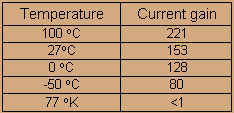 |
- The current gain varies significantly with temperature and drops to
less than unity at 77 K, which is the temperature of liquid nitrogen.
- Since liquid nitrogen is readily available at a very low cost, it is one of the most widely used methods of cooling a device. It is of interest to cool a BJT so as to remove excess heat from it. Circuits such as emitter coupled logic (ECL) consume lot of power and their scale of integration is limited by the ability to extract heat generated in the bipolar transistors. A ver simple method of overcoming this would have been to refrigerate the circuit in liquid nitrogen, but as we have seen, the current gain falls to less than unity, making the transistor useless.
- All the discussion regarding current gain so far has been for the
dc current gain. As we shall see later, the small signal current gain
is also of interest in many cases
The small signal gain is sometimes also called the ac gain because, the small signal is often a sinusoidal signal in many analysis.
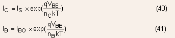
The small signal current gain can be expressed in terms of the dc current gain using the following general expressions for collector and base currents:
- The collector and base currents have ideality factors
 respectively.
The ideality factor may depart from unity at low or very high current
densities.
respectively.
The ideality factor may depart from unity at low or very high current
densities.
Using Eq. (39-41), we obtain
![]()
- The small signal current gain will be different from the dc gain if either the base or the collector ideality factor is different from unity.
- For example, at very low collector current densities, the base current
is dominated by SCR recombination current, which has an ideality factor
of 2. Since the collector current
has ideality factor of unity at low or moderate currents, the small signal current gain will be twice that of the dc gain. - At very high collector current densities, we shall see later, collector
current has ideality factor greater than unity, while the base current
has ideality factor of unity. In this case
the small signal gain will be smaller than the dc gain. - For intermediate collector current densities, the dc gain equals the small signal current gain.
![]()
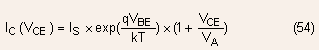
The collector current in active mode of operation for a uniformly doped
base is given by
the expression:
![]()
It appears from this equation as if the collector current is independent
of the collector- base voltage. However, this is not so because the effective
base width ![]() depends
on the
depends
on the
collector bias as illustrated by the Figure below:
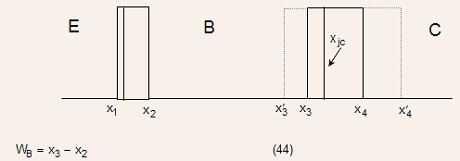
- As the collector-base voltage
 increases,
the depletion region associated with the collector base junction widens
as illustrated by the Figure above. The base width narrows to
increases,
the depletion region associated with the collector base junction widens
as illustrated by the Figure above. The base width narrows to  As
a result of the decrease in base width, the collector current would
increase. This base width modulation effect described first by James
Early, is known as the Early Effect.
As
a result of the decrease in base width, the collector current would
increase. This base width modulation effect described first by James
Early, is known as the Early Effect.
The change in collector current as a result of change in collector-base voltage can be evaluated using Eq. (43)
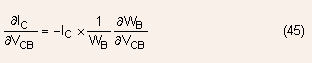
Using Eq. (44), we obtain
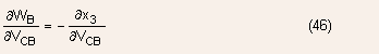
Using the expression for the magnitude of collector-base depletion charge, we can obtain the following results:
![]()
![]()
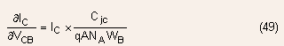
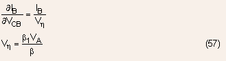
Defining a parameter called the Early voltage:
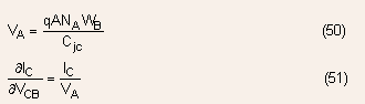
- The expression for early voltage shows that its value depends on the collector-base bias but this dependence is weak so that for collector-base voltages not far from zero:
![]()
Representing ![]() we
obtain
we
obtain
![]()
- Noting that
 and
base emitter voltage in active mode being less than unity is often much
smaller than the early voltage, we obtain
and
base emitter voltage in active mode being less than unity is often much
smaller than the early voltage, we obtain
Eq. (54) shows that the collector current would slowly increase with the collector-emitter voltage as illustrated by the Figure below:
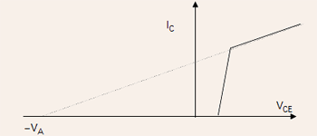
Through extrapolation of the characteristics in active mode, the early voltage can be measured!
| Impact of Early effect on Base current |
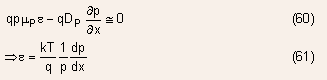
Ignoring the small reverse current of the collector-junction, the base current can be written as
![]()
Eq. (22) for ![]() show
that these currents have no dependence on the collector-base voltage so
that
show
that these currents have no dependence on the collector-base voltage so
that
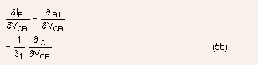
Use of Eq. (51) allows Eq. (56) to be re-written as:
Eq. (57) can be re-written in terms of the base transport factor
![]()
- Because of very small value of base transport factor, the voltage
 so
that the base current is much less affected by the applied collector
bias as compared to the
so
that the base current is much less affected by the applied collector
bias as compared to the
collector current.
Example 2.9 Determine the Early voltage for an NPN transistor
having the following characteristics at ![]() and
-5 Volts.
and
-5 Volts.
Take, ![]() base
doping of
base
doping of ![]() effective
base thickness of
effective
base thickness of ![]() collector
doping of
collector
doping of ![]()
Solution : The collector depletion width and junction capacitance/area can be calculated to be :
![]() The
early voltage then can be calculated to be:
The
early voltage then can be calculated to be: ![]()
![]() the
collector depletion width and junction capacitance become
the
collector depletion width and junction capacitance become ![]() The
new early voltage
The
new early voltage ![]()
| Non-Uniform Doping |
- In all the analysis carried out so far, the doping in emitter, base
and collector were all assumed to be uniform. However, in most devices,
due to the nature of fabrication,
doping in emitter and base is nonuniform, approximating gaussian or error function most of the time. We will next look at the model for collector current when base doping is
nonuniform.
- As a result of nonuniform base doping, an electric field is present
in the base so that the electron cannot be assumed to be simply diffusive.
The magnitude of the electric field
can be obtained through analysis of the hole current:
![]()
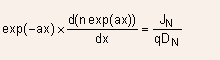
This hole current supplies the holes that are injected into the emitter or those that recombine in the base. If the hole current is assumed to be very small so that:
This expression for electric field can be used to write the expression for electron current or equivalently collector current as:
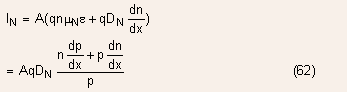
Eq. (62) can be re-written as
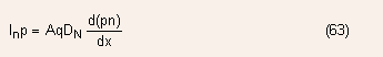
Integration of this equation across the base gives:
Since doping is nonuniform in the base, the mobility and therefore the
diffusion constant would also vary in the base. This variation, however,
is small and ![]() represents
its average value in the base.
represents
its average value in the base.
·The electron density at the edge of reverse biased collector-base
junction will be negligible so that ![]() and
the electron-hole product at the edge of emitter-base
and
the electron-hole product at the edge of emitter-base
junction can be written as :
![]()
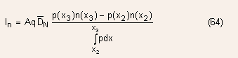
Eq. (64) can now be simplified to
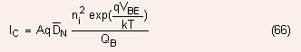

·Eq. (66) is known as the ![]() representation
of the collector current. A model forBJT will be derived using this equation
later on.
representation
of the collector current. A model forBJT will be derived using this equation
later on.
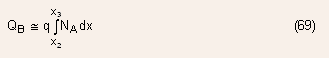
![]() is
known as the Gummel number for the base. Using quasi-neutrality condition
for the base:
is
known as the Gummel number for the base. Using quasi-neutrality condition
for the base:
![]()
For low level injection: ![]() so
that
so
that
For uniformly doped base :
![]()
Substitution of Eq. (70) in Eq. (66) gives the same expression for collector current as Eq. (1) that we have used throughout the previous analysis.
Example 2.10 (a) An NPN transistor has a nonuniform doping in the base
described by the expression :![]()
Assume that average diffusion constant in the base is ![]() and
that effective base thickness is
and
that effective base thickness is ![]() Determine
the magnitude and direction of electric field in the base
Determine
the magnitude and direction of electric field in the base
(b) Obtain an expression for electron density profile within the base
(c) Determine the injection efficiency limited current gain at room temperature.
Assume that
![]()
(a) Under low level injection conditions, ![]() so
that
so
that
![]()
The negative sign indicates that the field is directed towards emitter. It therefore aids in drift of electrons towards the base.
(b) The electron current density within the base can be written as
![]()
Using the expression for electric field obtained earlier, we can re-write the above expression as
![]()
This equation can be expressed as
Integration of the above expression from x to WB with the boundary condition that electron density at the collector end of the base is negligible, we obtain
![]()
(c) The expression for current gain can be modified to

For calculating the band gap narrowing in the base, we find the average doping in the base and use it in the expression given in the text. With that we obtain a current gain of 116.