| Introduction |
variety of applications
Our discussion of BJT characteristics will proceed in the following order:
(1) Basic characteristics of a BJT
(2) BJT in forward active mode of operation
(3) Dynamic characteristics of BJT in active mode
(4) High level injection effects
(5) Breakdown in BJT
(6) Circuit Models
(7) Design perspective
Most of our discussion will center around Silicon NPN transistor meant for high frequency applications.
The Figure below shows a simplified schematic of a planar npn transistor:
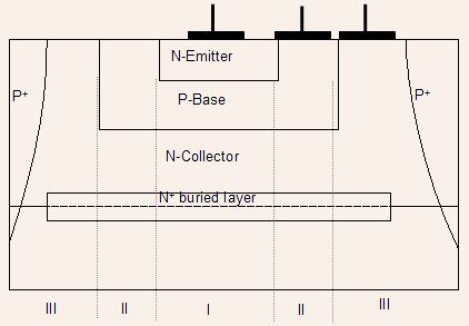
- The transistor is fabricated on an N-epilayer grown over a P-type
substrate. The P-type base is diffused first. The base diffusion depth
determines the thickness of the collector
region. - This is followed by + N emitter diffusion. This determines both the emitter thickness as well as the base thickness.
An + N buried layer is also used in the collector to reduce
the collector series resistance.
The contacts for all three layers are formed at the top.
- Since several transistors have to be fabricated on the same piece
of Silicon, there is a need for isolating each transistor from the
other. There are several ways of doing this, one
of which is junction isolation. This is done by creating a reverse biased junction between two transistors through diffusion of P-type impurity right down to the substrate.
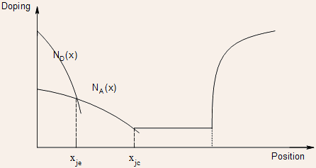
- The doping profile and the junctions are illustrated by the Figure below :
·
- In the schematic of the transistor, three distinct regions can be identified:
(i) Region I: this is known as the intrinsic transistor region where all the interesting things occur
(ii) Region II: this is known as the extrinsic collector-base region.
This region provides a contact to the base
(iii) Region III: this extrinsic collector region again serves the role
of providing a contact to the collector
- Since the transistor action occurs only in the intrinsic region,
the other two regions are called parasitic regions. One of the goals
in design of transistor is to minimize the area of
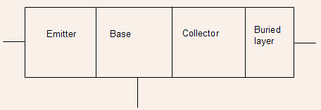
the parasitic regions to a minimum through process innovation. - In most of our discussions on BJT, we shall confine our attention to the intrinsictransistor region and model it simply as that shown below.
The structure of the transistor shows that there are two PN junctions within it; one at the emitter-base junction and the other at the collector-base junction.
- However, characteristics unique to a BJT cannot be obtained by simply
taking two PN junction diodes and externally connecting them as shown
below:
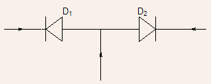
- In the circuit above, the two diodes do not interact with each other in the sense that their current-voltage characteristics when they are connected to each is same as that in isolation. If diode D1 is forward biased and D2 reverse biased, then all the current of D1 would flow through the base contact and D2 would be carrying only its reverse saturation current. The base current would be practically equal to the emitter current.
- Unlike the situation above, where the two diodes function in isolation of each other, the two PN junctions are closely coupled to each other as explained below:
- Consider the case where the base-emitter (EB) junction is forward biased and base collector junction (CB) junction reverse biased. This mode of operation is known as the forward active mode.
- At the EB- junction holes will be injected by the P-type base into the emitter and electrons will be injected by the N-type emitter into the base.
- The holes injected into the emitter would diffuse and get collected
at the emitter contact as expected. However, the electrons injected
into the base are not collected at the base contact, which is relatively
far away but most of the electrons diffuse to the much nearer CB-junction
from where the junction electric field sweeps them into the collector!
- As a result, a large current flows into the collector despite the reverse bias
- This is not strange, if it is remembered that in reverse bias electrons
are required to flow from P®N and holes from N®P and current
is small not because it is difficult for
carriers to move from one region to another due to any barrier but because there are so few electrons in P-region and holes in N-region.
- The forward biasing of the emitter base junction floods the P-region of the CB diode with electrons thereby increasing the current flow.
- The collector current would be determined primarily by the electrons injected into the base by the emitter, its own reverse current being extremely small.
- As expected, this current flowing through the reverse biased collector-base
junction will be little influenced by the collector-base voltage but
very sensitive to the emitter-base
voltage.
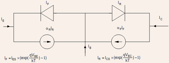
The transistor in forward active mode of operation can therefore be represented by the following circuit:
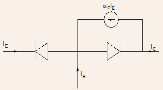
- Apart from the expected diodes, the Figure shows a current source
F F I a , which represents the fraction of emitter-base current that
is coupled into the collector-base
junction.
- As mentioned earlier, the collector current would be very sensitive to the emitter-base voltage and insensitive to collector-base voltage .
- We have a very interesting situation here of a current flowing between
pair of terminals being insensitive to changes in voltage across it
but very sensitive to voltage applied
across a different pair of terminals!
![]()
- Because of the prominence of transconductance or its inverse transresistance, the device is appropriately called a Transistor!
One of the tests for any three terminal device being called a transistor is :
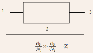
A rearrangement of this equation shows that a device which has much larger transconductance as compared to output conductance can exhibit voltage gain.
![]()
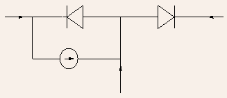
- Just as a fraction of current of forward biased emitter-base junction
gets coupled into the collector-base junction, similarly we have a
complimentary situation where current of
forward biased CB junction will also get coupled into reverse biased emitter-base junction in what is known as reverse active mode of operation.
The circuit representation for the reverse active mode would therefore be as shown by the Figure below :
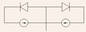
More generally, it may be expected that a transistor can be represented as :
Although the Ebers-Moll representation is a very general one, we shall for the sake of simplicity derive it under the following assumptions:
(i) 1D transistor structure with uniform doping in all the regions
(ii) Narrow base width so that carrier recombination within base can
be neglected
(iii) Low level injection condition in all the regions
(iv) SCR recombination is neglected
(v) Steady state conditions
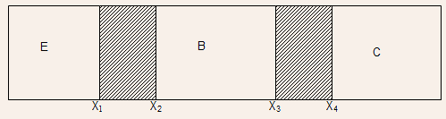
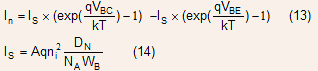
Using the results derived earlier for PN junctions, the emitter, base and collector currents can be expressed as
- The emitter and collector current are composed of electron and hole
currents flowing through their respective junctions. The base current
is due to holes injected into the
emitter and collector regions.
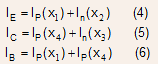
- The neglect of recombination within the base (assumption ii) means that the steady state electron continuity equation simply reduces to
![]()
In other words, electron current within the base is constant. All the electrons that are injected from the emitter reach the collector and viceversa.
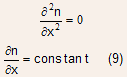
- Use of low level injection assumption means that the electron current in a uniformly doped base can be modeled as a diffusion current alone :
![]()
Substitution of Eq. (8) in Eq. (7) gives
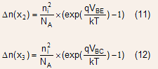
The electron density varies linearly within the base so that :
![]()
The excess electron densities at the two ends of the base can be expressed as :
The electron current can therefore, be written as :
Without going into the details, the hole current injected into the emitter being proportional to the excess hole density in the emitter, can be written as :
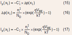
The negative sign indicates that the current is in negative direction.
Similarly, the hole current injected into the collector can be written as :
![]()
Using Eq. (4-18), the emitter and collector currents can be expressed as :
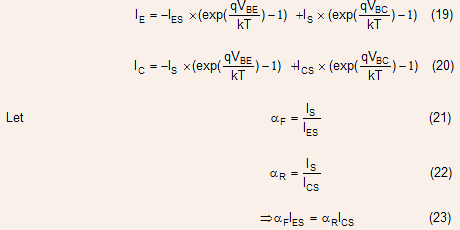
With these definitions, the Ebers-Moll can be expressed in terms of the following two equations :
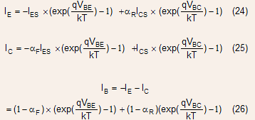
Eq. (24-26) can be represented by an equivalent circuit shown below :
The model shows that current flowing through each junction is made of two components :
(i) Normal diode current
(ii) Current due to coupling of a fraction of current flowing in the
neighboring diode.
The Ebers-Moll Model can be used to understand transistor operation in all four modes of operation depicted below :
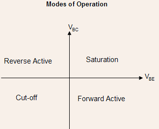
As shown by the diagram, there are four modes in which a BJT can be operated :
(i) Forward active Mode: The emitter-base junction is forward biased and collector-base junction is reverse biased.
(ii) Saturation Mode: Both the junctions are forward biased
(iii) Reverse active Mode: The collector-base junction is forward biased
and
emitter-base junction reverse biased.
- The forward active mode of operation is the most important region
of transistor
operation and will be discussed in detail in the next few lectures. This would be followed
by a discussion of characteristics of BJT in cutoff and then saturation.
Example 1.1 : The electron density within the base of a uniformly dopde NPN BJT is constant as shown below :
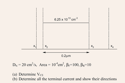
Solution : (a) It is obvious that substantial minority carrier injection
has taken place from both the junctions so that both are forward biased
and the transistor is in saturation.
(b) Since the electron current in the base is given by the expression
![]() N
it is zero because the electron density is constant. Let us calculate
the hole current IP(x1), injected into the emitter. Using the definition
of forward current gain :
N
it is zero because the electron density is constant. Let us calculate
the hole current IP(x1), injected into the emitter. Using the definition
of forward current gain :
![]() forward
active mode.
forward
active mode.
To use this expression, we have to calculate the electron current for
the same emitter-base forward bias as the present case but the transistor
in active mode. In that case, ![]() remains
the same but
remains
the same but
![]() so
that
so
that
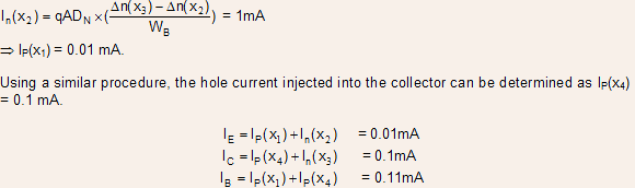
n the calculations above, we have used only the magnitudes of the currents
into account.The emitter current being composed of hole injection into
the emitter would be negative,
for the convention that current entering a terminal is taken as positive.
Similarly the collector current would be negative and only the base
current would be positive.
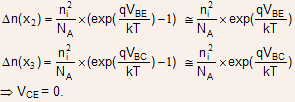
Example 1.2 : Determine the collector-emitter voltage of the transistor shown below with its collector open circuited.
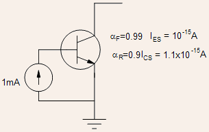
Using the Ebers-Moll model we obtain
![]()
Since 1mA current is flowing through the base and emitter terminals,
the emitter-base
junction is obviously forward biased so that ![]()
Using the expression derived above, it is also clear that collector-base
junction will also be forward biased so that ![]() kT
kT
This simplification along with Eq. (a1) allows the collector-emitter
voltage to be expressed as![]()
Using the reciprocity relationship : ![]() we
obtain the final expression as
we
obtain the final expression as ![]()