| Semiconductor as a device |
| |
| |
| 5.4 Metal-semiconductor diodes (Schottky barrier diode): |
| |
| |
A metal-semiconductor barrier, under special condition, is capable of electro-optic
nonlinear effects. Basic design of Schottky junction barrier is defined as a difference between the conduction bands
of semiconductor to the metal Fermi level. In ideal situation, the barrier height is defined as
|
|
Where Φm metal work function and χs
is the electron affinity of semiconductor.
|
The potential, or the built-in potential is
|
|
Net current with the applied bias is 
|
| |
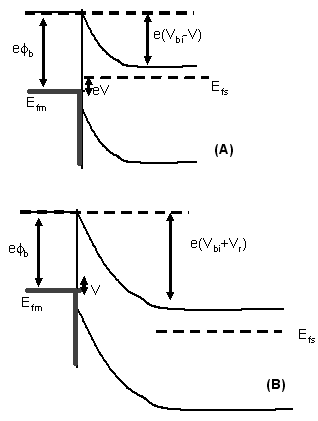 Fig.4.11 Schottky diode (A) forward and (B) reverse bias; Some facts about
metals and semiconductor used in Schottky diodes. |
| Work functions of some metals |
| Element |
Work function , Φm (volt) |
| Ag, Silver |
4.26 |
| Al, Aluminium |
4.28 |
| Au, Gold |
5.1 |
| Cr, Chromium |
4.5 |
| Mo, Molybdenum |
4.6 |
| Ni, Nickel |
5.15 |
| Pd, Palladium |
5.12 |
| Pt, Platinum |
5.65 |
| Ti, Titanium |
4.33 |
| W, Tungsten |
4.55 |
Electron affinity of some semiconductors
|
| Element |
Electron affinity, χ (volts) |
| Ge, Germanium |
4.13 |
| Si, Silicon |
4.01 |
| GaAs, Gallium Arsenide |
4.07 |
| AlAs, Aluminium Arsenide |
3.5 |
|
| |
| |
Some remarks about the Schottky barrier:
|
1. Schottky diode is formed by placing a thin film of metal in direct
contact with a semiconductor. The metal film is usually deposited on an n-type semiconductor.
2. Switch-on voltage is low, 0.3~0.4V ( regular diode: 0.7~1.5V)
3. Reverse leakage current, Is, is larger than p-n junction diodes.
4. Breakdown voltage is small.
5. Fast switching times than p-n junction diode.
6. Schottky diodes are majority carrier devices.
7. The depletion layer is thinner than that of a p-n diode and hence has larger reverse current .
8. There might be a problem of contact between the metal and semiconductors. The main reason is lattice mismatching.
People also use conducting oxide ( ike ITO, tin titanium oxide) as alternative.
|
| |
| |
| 5.5 Hetero Junction diodes: |
| |
| |
Till now you have seen the same material is differently doped attached to form a
p-n-junction and observed the current nonlinear flow. In another case, you have seen two very different classes of
materials (metals and semiconductors) being in contact to form a device. Our journey is not going to stop here;
we will go further and see how two different semiconductors could form a junction. Such junctions are called hetero
junctions. The best example is GaAs and AlGaAs diode.
|
|
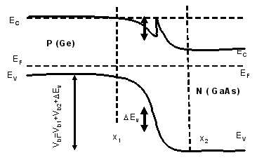
Fig.4.12 energy band diagram of n- hetero junction |
| |
Assume two materials having different band gaps (Eg1 and Eg2) and different dielectric
constants (ε1 and ε2), then we can visualize the band diagrams at thermal equilibrium as follows. Typical energy band
diagram of n-n type hetero junctions are given in fig 4.12 . Similarly p-n and p-p hetero junctions are also in practice.
Hetero junctions are mostly used in photonic applications as, light emitting diodes (LED), diode laser, photo-detectors
and solar cells.
|
In hetero junctions, unlike homo junctions, conduction band edges ( ΔEc)
and valence band edges ( ΔEv) discontinuity is invariant, to match Fermi level to be in equilibrium. Hence
the built-in potential is different for the two sides. So the total Vbi=Vbi1+Vbi2.
|
The current voltage relationship is
|
|
This expression is different to that of other junctions mentioned previously.
Here the current is totally temperature dependent. Moreover, the reverse current never saturates, but increases
linearly with voltage.
The hetero junctions were very popular because of technology availability to design lattice-matching junctions
without any interface traps. We will see how hetero junctions are used as photonic devices.
|
| |
| |
| 5.6 Photodiode: |
| |
| |
These hetero junctions are used in detecting light intensity. Essentially the principle
is to convert conversion of optical signal into electrical signal. This can be visualized as the optical
absorption creating an electron hole pair which creates carrier transport and hence the current. You might have
had information about continuous lasers and pulsed lasers. In pulsed laser, the pulse rates vary from nano,
femto pico seconds. The diode, which we use, must be capable of responding in those time domains.
The current expression in photodiode is directly proportional to the light intensity as well as photon energy.
Keep in mind that the photo diode has to be selected according to the wavelength region of interest. That means the
band gap of the diode material must match with the desired light energy.
|
|
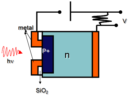
Fig 4.13 Typical configuration of a photodiode
|
|
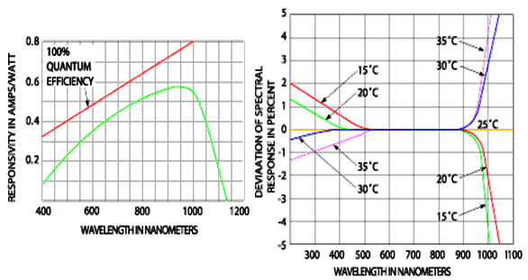
Fig. 4.14 Si photo diode responsivity and temperature response
|
| |
The primary demands of photo diode are
|
1. High efficiency, and responsivity to convert efficiently the optical signals
to electrical signal
2. Selective operating region: (For example, the communication wavelengths 1.30 and 1.55μm. These wavelengths are dependent
on the optical fibre low attenuation and low dispersion region)
3. High electrical bandwidth and low signal to noise ratio (data rate = frequency/0.8)
4. Detector-geometry must be compatible to the fiber geometry
|
Other than just simple pn diode based detectors, we may have:
|
PIN-Photodiodes: In reverse-biased p-n-photodiodes e-h-pairs are generated by
photon absorption in the depletion layer; electrons and holes move in the bias field in opposite directions to the
n and p-contacts. (PIN means, p-n junction with depletion layer arranged according to the intensity distribution)
|
Avalanche Photodiodes: p-n-photodiode, where the primary e-h-pairs are multiplied
internally by impact-ionization in high field regions of the APD.
|
| |
| |
| 5.7 Light emitting diodes (LED): |
| |
| |
It is one of the simplest devices, which is very important as a display device
as well as optical signal communicator. The light emitting diode (LED) is a design wherein electrical energy creates
e-h pairs and the recombination is a radiative process leading to electroluminescence. Here the fabrication is also
relatively simple, to that of semiconductor laser, as we don’t need any cavity arrangement to boost the
spontaneous emission.
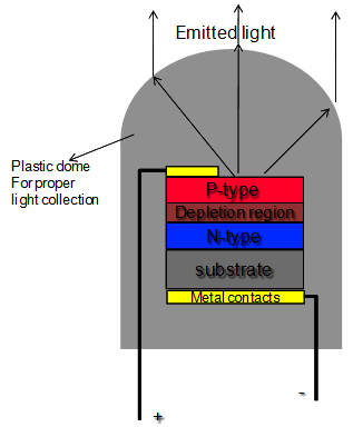
The basic LED is a p-n junction in which the operation is in forward bias. In the forward bias we are injecting
electrons and holes into p and n sides respectively. Injected carriers recombine radiatively with the majority
charges in the depletion layer. Remember, in indirect band gap semiconductors light emission is very
poor compared to direct band gap.
|
| |
|
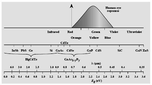
Fig.4.15 Demands of Photonics
Semiconductor band gaps in the UV-VIS and IR region
|
Typical materials used are semiconductor alloys such as AlGaAs and GaAs/GaP.
(Remember: The band gap in these alloys change from direct band gap to indirect when the percentage of AlAs
( or GaP) is more than approximately 0.5).
|
The LED emission is quite dependent on the band gap and the band gap vs region
of emission is given in figure 4.15. Much of radiative processes in semiconductors are given in chapter 3.
|
|
Fig.4.16. Typical simple Light emitting diode (LED. Where plastic dome enclosure is
issued to maximise the collection of the emitted light from LED.
|
| |
There are many varieties in the design in the recent past: hetero junction
LED (choosing two diverse materials), edge emitting LED (for better coupling of light into fibres) and surface
emitting LED (directly attached to a fibre and with the increased efficiency by incorporating micro-lens geometry) .
That’s all for this course, but if you wish you can study more about LED in your applied courses.
|
| |
| |
| |
| |
| 5.8 Semiconductor Laser Diodes: |
| |
| |
A laser diode principle is same as the conventional laser: an active layer is
contained in between two highly reflecting mirrors. A detailed information on the working principles of lasers,
you might have had in your laser course. Here the p-n junction, just like the LED acts as source of light.
Here three things one should keep in mind
(1) the emitted light has to be stimulated emission,
(2) the stimulated emission has to be amplified and
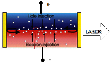
(3) For amplification purpose, you need cavity ( imagine the emitted
light is in between two mirrors as shown in Fig 4.17)for amplification purpose.
|
|
Fig.4.17 Semiconductor laser diode and schematic arrangement of layers.
|
In general, for laser action to take place, population inversion and optical
feedback are necessary. Population inversion is achieved by passing a high drive current through the diode, which
results in the majority charge carriers to excite to a higher energy level.
The electrically driven stimulated emission, as mentioned in the previous lectures, is highly confined in the
optical waveguide formed by the refractive index contrast between the active medium and the reflectors
(let us call them as clad layers). Other diode laser structures are quantum well lasers and vertical cavity
surface emitting lasers.
|
| |
| |
Table 5.4.1 |
| Important semiconductor laser materials |
| Compound |
Wavelengths (nm) |
Notes |
| GaN |
<400 -> |
1995 |
| ZnSe |
460-530 |
first demonstrated 1991 |
| AlGalnP |
630-680 |
|
| Ga0.5ln0.5P |
670 |
active layer between AlGalnP layers;
long room temperature lifetime |
| Ga1-xAlxAs |
620-895 |
x=0 to 0.45; lifetimes very short for wavelengths below 720 nm |
| GaAs |
904 |
|
| ln0.2Ga0.8As |
980 |
strained layer on GaAs substrate |
| ln1-xGaxAsyP1-y |
1100-1650 |
lnP substrate |
| ln0.73Ga0.27As0.58P0.42 |
1310 |
major fiber-communication wavelength |
| ln0.58Ga0.42As0.9P0.1 |
1550 |
major fiber-communication wavelength |
| lnGaAsSb |
1700-4400 |
possible range, developmental,on GaSb substrate |
| PbEuSeTe |
3300-5800 |
cryogenic |
| PbSSe |
4200-8000 |
cryogenic |
| PbSnTe |
6300-29000 |
cryogenic |
| PbSnSe |
8000-29000 |
cryogenic |
|
| |
| Diode lasers are often unstable because of junction temperatures, current noise,
and the perturbation of the external cavity length used for narrowing the laser spectrum. Moreover, the power output
is limited to several watts in Continuous operation mode because of the very small geometries. |
| |
| |
| |
| |
| |
| |
| |
| |
| |
| |