| Semiconductor as a device |
| |
| |
| 5.3 Principles of p-n junctions4 (homo-junctions): |
| |
The basic technological concept behind setting up p-n junctions is to diffuse or
implant electron deficient (holes) or electron rich (electrons) impurities in an n or p-type pre-doped semiconductor,
respectively. Schematic representation of a p-n junction is given in figure 4.4. Carrier concentration profile from
p region to n region is estimated in two ways: abrupt and graded junctions. When n-doped and p-doped pieces of
semiconductor are placed together to form a junction, electrons migrate into the p-side and holes migrate into
the n-side. Departure of an electron from the n-side to the p-side leaves a positive donor ion behind on the
n-side, and likewise the hole leaves a negative acceptor ion on the P-side. This creates a space charge region
which is electrically neutral between the junction causing an intermediate width called depletion layer.
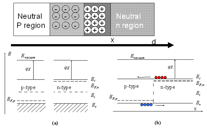
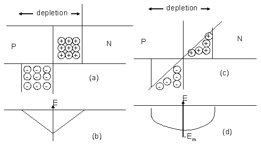
Fig 4.4 explains the neutral p-type and n-type junction formation. The leftmost and rightmost side p and n type regions are
having flat energy band diagrams. Notice the corresponding Fermi energy levels of donors and acceptors
(as learnt in chap 1).
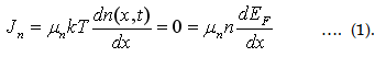
To reach the thermal equilibrium, both electrons and holes close to the active region of the junction diffuse across
the junction into the p-type/n-type region, respectively.
|
| |
|
Fig 4.4. Schematic representation of a p-n junction; (a) before and (a) after p-n junction formation
|
| |
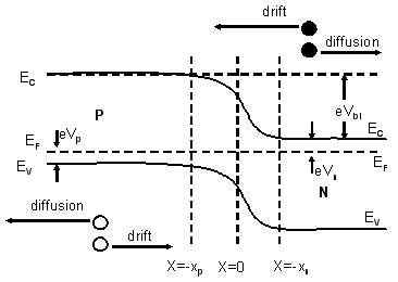
This process leaves the ionized donors (acceptors) behind, creating a region around the junction, which is
depleted of mobile carriers. We call this region the depletion region, extending from x = -xp to x = +xn. The charge
due to the ionized donors and acceptors causes an electric field, which in turn causes a drift of carriers in the
opposite direction. The diffusion of carriers continues until the drift current balances the diffusion current,
thereby reaching thermal equilibrium as indicated by a constant Fermi energy. The thermal equilibrium schematic
energy levels are given in figure 4.5.
Electron drift and diffusion are in opposite direction (diffusion takes place from n-type to p-type). Similar
is the case for holes with directions reversed.
|
| |
|
Fig.4.5 Energy diagram of p-n junction at thermal equilibrium |
| |
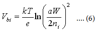
Note that while in thermal equilibrium, no external voltage is applied between the
n-type and p-type material but there is an internal potential, Vbi, which is caused by the work function difference
between the n-type and p-type semiconductors. This potential is called the built-in potential. Here we have to
consider two cases as mentioned before: abrupt and graded junction.
|
One would imagine that the concentration of both p type and n type impurity
concentrations: donor (Nd) and acceptor (NA) changes abruptly. For simplicity let us consider one sided abrupt
junction (Nd << NA) denoted as p+n junction.
Let us consider the situation of thermal equilibrium (for time being, assume there is no carrier
recombination process involved) and recall the current expression involving drift and diffusion processes
from chapter 2
Eq28 and Eq20 (for Fermi level expression)
|
|
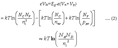
that means to achieve thermal equilibrium in the p-n junction, Fermi level must
be constant through out the device. From the diagram, the built-in potential can be written as (remember we are
dealing homo -junction, hence the same band gap Eg)
|
|
This is because at equilibrium 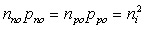 (product of majority ( electrons) and minorities ( holes) )
in n type, and similarly for p type) (product of majority ( electrons) and minorities ( holes) )
in n type, and similarly for p type)
|
Rewriting 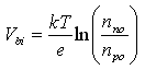 and/or and/or 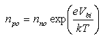 similarly for holes
.(3) similarly for holes
.(3)
|
The above relations give insight into the carrier concentration distribution and the
built-in potential at the junction.
For the width of the depletion layer, one has to take the Poissons relations (lecture notes Eq. 36) and integrating between
the boundary values between xp>> 0 << xn.
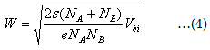
The width of the depletion layer comes out to be
|
|
and for one sided abrupt junction it is 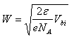
|
One can also write the same equation, considering majority carrier distribution also,
which is more accurate than Eq4.
|
|
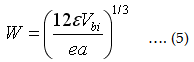
Junction diode depletion layer capacitance per unit area is defined as the ratio
between the dielectric susceptibility ( εs) to the depletion layer width. This was derived from the fundamental
definitions of the capacitance. Capacitance measurement is one way of evaluating impurity
concentration levels.
|
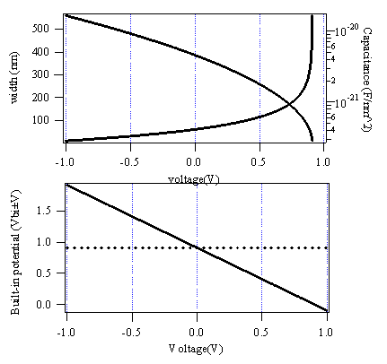
The values of built-in potential, depletion layer width and capacitance
are plotted against the bias voltage in the figure 4.6. You will see that width is narrow in forward bias
whereas it expands quite rapidly in negative bias. Whereas capacitance varies exponentially with the applied
bias. Such changes in the capacitance of the p-n diode are applied in many of the circuit applications, as
a voltage variable (convert Width into bias voltage!!) capacitor (or varactor).
|
| |
| |
| (a) Linearly graded junction: |
| |
Here the impurities are linearly graded, that means the distribution is linear.
|
|
Fig4.6. abrupt and graded junctions (a & c) space-charge distribution and (b&d)
field potential variation ; ( bottom ) depletion layer width, capacitance and built-in potential variation
with applied voltage.
|
Here consider the distribution is linear between the limits -W/2 and W/2 with a
linear coefficient of a. Once again integrating the Poissons equations between the above limits we get
the expression of depletion layer width as
|
|
and
|
|
| |
| |
| (b) Current flow: ideal condition: |
| |
| |
Now we know how a p-n junction band diagrams are modified with the applied bias.
We also observed the carrier concentration dependence on the band diagram under thermal equilibrium. But still we
have not considered how the mobility of carriers further influences the current voltage characteristics. In our
earlier sections we came to know about various current inducing components: drift, diffusion and electron-hole
recombination processes that influence over-all transport in semiconductors (section 3.4). Now here we will
examine the various current sources with respect to components applied bias voltage changes. Unlike metals,
semiconductors behavior is quite nonlinear and hence established as a potential electronic device.
During our calculation, we generally need to know the carrier density and the electric field distribution through
out the diode, which in turn can be used in evaluating the drift and diffusion currents. However, that requires
precise knowledge of Fermi energies, again if the currents are known. Hence, for obtaining an analytical solution
we will assume the following. Once we fix our assumptions, we can directly go to our equations of Chapter 1 and
Chapter 2 for obtaining the current solutions.
|
- Depletion layer has abrupt edge and the adjacent n-type and p-type are neutral regions.
- Carrier densities are related to electrostatic potential difference (Vbi) across the junction.
- Under the applied bias, the majority carrier densities are negligibly changed at the boundaries of the neutral region.
- None of the electron-hole processes (generation and recombination) would happen in the depletion region.
|
Under these, so called ideal conditions, no current is generated within the
depletion region and all current is coming from the neutral region.
|
You might have noticed from Eq.3 ( ) that the electron(hole) densities in the
neutral region are related to Vbi under thermal equilibrium (no bias). Under our assumptions it also holds even
for bias condition where Vbi-V is for forward and Vbi-V for reverse.
At low injection levels, injected minorities are very much less than the majority carrier densities.
|
Hence at the boundaries of depletion region ( x=-xm), 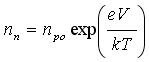
|
Similarly at x=xm, 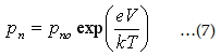
|
Thus the above relations gives us the minority carried densities at the boundaries
of depletion region (see fig 4.5, if you cant recollect the boundaries).
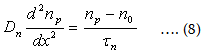
Under our next assumption there is no current flow within in the depletion region. We have to again go back to
our continuity equations (Eq30 of chapter 3), under steady state,
|
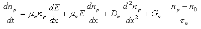 which will be reduced to which will be reduced to
|
|
Using the above bounder condition at x=-xm, and rearranging terms, we obtain
|
|
Where  , which is known as diffusion length of electrons. , which is known as diffusion length of electrons.
|
Similarly we also can write for holes,
|
|
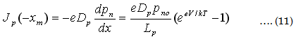
Hence the current expression for the boundary x=-xm, is
|
|
And
|
|
The total current obviously the sum of currents at both the boundaries,
|
|
Where 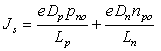
|
Equation 13 is the I-V characteristic feature of ideal diode. Figure 4.7 is the plot of
the I-V features of above relation. In the forward bias, the rate of current density increase is constant for V>3kT/e,
whereas in the reverse bias, the current saturates at -Js.
Now we come back from unrealistic assumptions, we introduce
the recombination-generation currents into the depletion region. Here we have to consider the real situation,
where we must consider the traps associated with defects or impurities. Recall about two different possible
recombination mechanisms: band-to-band recombination and Shockley-Hall-Read recombination.
|
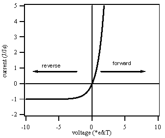 Fig4.7. Ideal diode I-V characteristics
|
| |
The recombination current is now JR = eWRt,
where Rt is the recombination rate (see section 3.3 of chapter 3)
|
We can write down the current due to the recombination as (for forward bias)
|
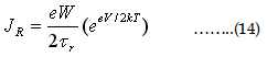
|
where effective recombination lifetime 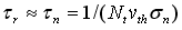 . .
|
Eq.14 sums up with the Eq.13 to give resultant forward bias.
|
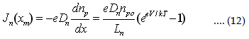
In general we can write forward bias current as 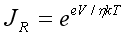 , where η is The ideality factor,
which can also be obtained from the slope of the curve on a semi-logarithmic scales. At several stages of η the
I-V characteristics are dominant by the factors as cited in the figure 4.8. , where η is The ideality factor,
which can also be obtained from the slope of the curve on a semi-logarithmic scales. At several stages of η the
I-V characteristics are dominant by the factors as cited in the figure 4.8.
|
|
Fig4.8. Real diode I-V characteristics at forward bias |
| |
| |
| (c) Reverse bias- Breakdown: |
| |
| |
Till now we have seen how a p-n junction operates under forward bias, where the I-V
characteristics are quite nonlinear. Let us now switch the direction of flow from forward to reverse.
The limitation of the maximum reverse bias voltage that can be applied to a p-n diode is called breakdown limit.
The breakdown is visualized as the rapid increase of the current under reverse bias. The breakdown voltage is a
key parameter of power devices. The breakdown of logic devices is equally important: as the device dimensions
are greatly reduced without reducing the applied voltage thereby increasing the internal electric field. Two
mechanisms can typically cause breakdown,
(1) Avalanche multiplication and
(2) Quantum mechanical tunneling of carriers through the band gap (tunneling effects).
Device people are happy to observe that both the processes are reversible, means without any physical damage.
However, keep in mind that the breakdown currents produce immense heating and hence cooling systems are highly necessary.
Let us briefly visit the two mechanisms
|
| |
| (i) Avalanche breakdown: |
| |
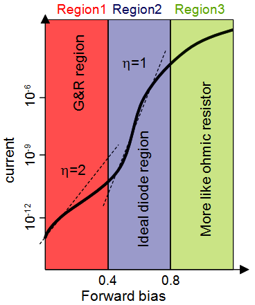
Avalanche breakdown is nothing but the impact ionization that produces additional
carriers in the electron hole pair generation/recombination. This we have dealt in our previous lessons.
This process happens in the depletion layer. Thermally generated electron in the depletion region gains the
kinetic energy from the electric field and if the field is sufficiently high, the high-energy electron knocks
out another electron to create electron-hole pair (Fig4.9). These newly created carriers, again gain kinetic
energy and produce additional e-h pairs. This process continues and is therefore called avalanche effect.
We had extensive over view of high field effects on the mobility carriers in the semiconductors in chapter 2. By knowing
the critical electric field (Ec), which can be calculated from the absorption coefficients of electrons and holes,
(see Fig 2.25 of chapter 2), one can estimate for abrupt junctions.
|
|
| Fig.4.9 Avalanche effect and critical fields in abrupt junctions
in Si, and GaAs
|
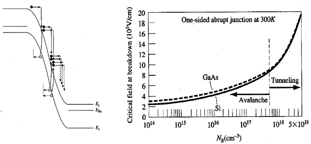
With the prior critical field values, we can estimate the Breakdown voltage VB as
|
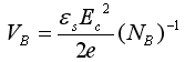 for abrupt junctions .......(15) for abrupt junctions .......(15)
|
and 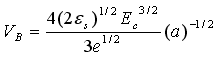 for linearly varying junctions
. (16) for linearly varying junctions
. (16)
|
It is clear from the above figures that the break down voltage approximations in
abrupt junctions is dependent on concentrations of lightly doped side and in linear junctions is dependent on linear
coefficient. In both the cases, larger the band gap is the larger the break down voltage.
|
|
Fig. 4.10. Avalanche break down voltages vs impurity/dopant
concentration (NB) and impurity gradient (a) in both abrupt and linearly graded pn-junctions
|
| |
| |
| (i) Avalanche breakdown: |
| |
| |
Quantum mechanical tunneling of carriers through the band gap is the dominant
breakdown mechanism for highly doped p-n junctions. The analysis is identical to that of tunneling in a semiconductor
where the tunneling is between the energy band gaps of the material.
Basically the tunneling process in semiconductor is a usual problem dealt in quantum mechanical fundamental problems,
where a wave function interacts with the periodic potential. Under very high fields, it is the process, where one
electron takes a transition from valance band to conduction band.
If you look back our high field mobility part in Chapter 2, we see that typically fields for Si and Ge are in the order
of 106 V/cm or higher.
|
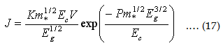
The tunneling current in p-n junction is
|
|
Where Ec is the electric field at the junction, Eg is band gap and m* is effective mass,
K and P are constants. When the fields approach 106, then there is a diffusion of electrons from band-to-band.
To create such a high field, both junctions must be heavily doped.
|
Let us give some landmarks for the two mechanisms that causes break down:
If the breakdown voltage is less than 4Eg/e, then it is due to tunneling effect. If the break down happens excess
of 6Eg/e then it is avalanche effect. The intermediate is the mix of both effects.
|
| |
| |
| |
| |
| |
| |
| |
| |
| |
| |