| Semiconductor as a device |
| |
| |
| 5.1 Introduction |
| |
In your previous lessons you have examined the electronic band structures and considered
carrier concentration and it’s effects on the electron-electron and/or electron – photon interactions in semiconductors.
Now we will extend our basics to understand the real semiconductor devices. There are many excellent semiconductor
devices that are available to you now and it is very hard to give emphasis to all. Our aim is to understand the
semiconductor basics and the functionality of semiconductor as a device. Hence, we very briefly take up few kinds
of devices and see if we can understand the functionality as well as basic material characteristics implemented
in their performance. One can always explore the semiconductor device applications out of their own interest.
|
Our coverage area is
|
- p-n junctions, both homo and hetero junctions: as a electrical and photonic devices.
- metal-semiconductor junctions
|
| |
We will try to examine the basic phenomena that control the semiconductor devices
and how a material property is exploited in the performance of a device. There is no need to mention the importance of
the semiconductor devices. The span of applications is widespread; information reception (diodes, transistors, detectors),
information generation ( microwave devices and diode lasers) and display ( LEDs).
|
|
| |
| |
| p-n junctions : |
| |
Basically, semiconductor properties are very fascinating, in the sense that its
physical properties can be widely changed by altering temperature or by doping. One would really expect a material,
which can change its total characteristic features, for example conducting to non-conducting. Another demand is
nonlinear behaviour: current will flow in one direction and in another direction it should not. In all these
scenarios semiconductors are flexible in realising such demands, either by themselves or by logically attached
to other semiconductor, oxide or a metal. Here will see how the properties (such as current flow ) could be
modified when the semiconductors in which the dopant is added across a boundary to create junction between two
diverse nature of the same semiconductors. In these junctions we manipulate our doping from p type to n type via
a region and hence named as p-n junction. This junction is having strong nonlinear effects and rectifying properties.
Many kinds of applications could be realised such as rectifiers, lasers, detectors etc, from p-n junctions.
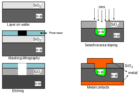
A schematic representation of the fabrication methodology for the fabrication of a p-n junction
is given in figure 4.1.
|
| |
|
Fig.4.1 Schematic representation of p-n diode fabrication process
|
| |
| |
| |
| |
| |
| |
| |
| |