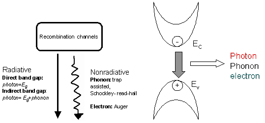
| Radiative and nonradiative recombination process |
| |
| |
| |
| |
| 4.3 Radiative and nonradiative recombination process |
Till now we considered various cases of electron hole pair generation, which is how an
electron transports in band-band or intraband transitions. Now let us see how the generated electron recaptures
with a hole. As mentioned in the introduction, the recombination of electron could be classified into three major
categories:
(1) band to band recombination, emitting a photon (radiative),
(2) recombination by means of simply
giving away energy to phonons and
(3) recombination by transferring kinetic energy to another electron and knocking
out into higher energy levels.
|
| |
|
| |
| |
| 4.3.1 Radiative recombination |
| |
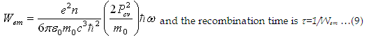
This Band-to-band recombination happens when an electron moves from its conduction band state to
the empty valence band state associated with the hole. The radiative recombination is a very important feature in
semiconductor optoelectronics. The generation and recombination rates are interrelated as both processes follow the
same path . The recombination rate is given by
|
|
Eq9 is born out of our previous discussion where the electron generation and
|
|
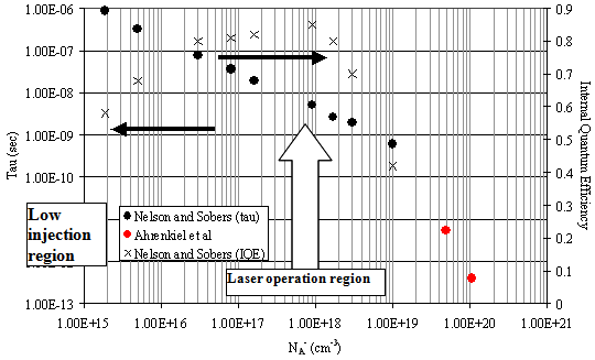
Fig3.10 Radiative life times and efficiency of p-doped GaAs vs Carrier concentration
|
| |
recombination occurred between two initial and final momentum vectors Ki and Kf. ( see Eq.1-3).
Let us recap again, the absorption states are 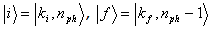 , and emission states , and emission states , However, the situation is not simple in
semiconductors. Here we have several exceptions (for example, the presence of forbidden gap impurity levels and lattice
related defect centers) those disobey the above general rule. In general, the absorption is followed by both radiative
and nonradiative recombinations. The radiative recombination could be both spontaneous ( initial and final photon are
incoherent) and stimulated (both photons are in phase). , However, the situation is not simple in
semiconductors. Here we have several exceptions (for example, the presence of forbidden gap impurity levels and lattice
related defect centers) those disobey the above general rule. In general, the absorption is followed by both radiative
and nonradiative recombinations. The radiative recombination could be both spontaneous ( initial and final photon are
incoherent) and stimulated (both photons are in phase).
|
The spontaneous radiate recombination rate, without any further discussion, given as
|
|
integration over  is needed to count the photons in 3D to get the rates for all the occupied
and hole states. here is needed to count the photons in 3D to get the rates for all the occupied
and hole states. here  , Fermi functions of electrons holes and respective representations of f(E) and reduced
density of states Ncv are given in Eq.2. , Fermi functions of electrons holes and respective representations of f(E) and reduced
density of states Ncv are given in Eq.2.
Here the Eq10, takes different conductions depending of carrier injection (optical, electrical or thermal).
|
| (i) Minority carrier injection: |
If the electron density is greater than hole density, then fe(Ee) is almost unity and the
radiative rate is 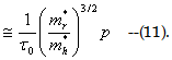 This means the radiative rates are proportional to the minority carrier densities. This means the radiative rates are proportional to the minority carrier densities.
|
| (ii) Strong injection: |
In this case very high densities of both electrons and holes are injected. In that case,
both Fermi functions could be treated as very sharp functions and hence the radiative rate is 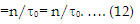
|
| (iii) Weak injection: |
Here we can write the Fermi functions in terms of Boltzmann distribution. Then rates turns
out as  where where  If we turn the total charge (n or p) as n+ Δn (similarly for p) then we will have
the radiative rates for excess carrier concentration as If we turn the total charge (n or p) as n+ Δn (similarly for p) then we will have
the radiative rates for excess carrier concentration as  This condition suggests that for
low injection, the radiative life times (1/Rsp) are much smaller than This condition suggests that for
low injection, the radiative life times (1/Rsp) are much smaller than  . Means electrons have much less probability
to find a hole to recombine. . Means electrons have much less probability
to find a hole to recombine.
|
| (iv) Inversion : |
If the sum of both densities is equal to one , then the radiative rate is equal to  or .
This is typically the threshold condition for a semiconductor diode laser. or .
This is typically the threshold condition for a semiconductor diode laser.
|
| Gain: |
Though it is not totally relevant here, for the sake of continuity, we have to see how
these radiative transitions turn into mega-light amplifiers, ie., lasers. Prerequisite for a laser material is to have
optical gain. In normal conditions, an electron travels from valence band to conduction band by absorbing a photon.
If we assume a condition where the valence band if fully empty and conduction band is rich of electrons? . This happens
only when we continuously pump electrons (population inversion). At this situation more number of photons are emitted
than absorbed. This nonlinear phenomenon is called stimulated emission and the coefficient is called optical gain. This
is simply the difference between the emission coefficient and the absorption coefficient. If the value is positive, then
the material is gaining otherwise, loss. The gain and loss vary with the input power of injection of carriers. If we
assume as 1-D system, the gain (g) and loss ( α) are related to emission as
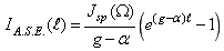 . Keep in mind that the gain spectrum is at
higher energy side to the emission spectrum. . Keep in mind that the gain spectrum is at
higher energy side to the emission spectrum.
|
Table 4.3.1 |
| Table 1 Gain cross section per quantum dot/ nanocrystal determined for various material systems |
| Quantum dot material |
Net modal gain (cm-1) |
Net Material gain (x 104cm-1) |
Areal dot density (Cm-2) |
Active layer thickness(nm) |
Filling factor (x10-4) |
Gain cross section per dot(x10-16cm-2) |
Reference |
| InAs Single QD layer |
8.2 |
9* |
1x10¹¹ |
1.7 |
1.2 |
1200 |
16 |
| InAs 7 QD Stacks |
70-85 |
1.5* |
1x10¹¹ |
100 |
48 |
4000 |
17 |
| GaAs Single QD layer |
13* |
|
1x10¹⁰ |
|
|
450* |
18 |
| Si NS |
100 |
1 |
2x10¹⁴ |
100 |
970 |
0.5-5 |
This Work |
| Calculated Approximately |
** http://prakash.iitd.ac.in/pub.htm |
|
Here we have considered that only the conduction and valence bands are responsible for
radiative transitions. However, in some exceptional cases, it is also possible to turn the intermediate levels
(such as impurity levels or defect levels) as radiative centers. This one can be visualized as the energy transfer
between two radiative systems, where the end -emitter is at minority level (for example see the literature for
Silicon nanocrystals and Erbium).
|
| |
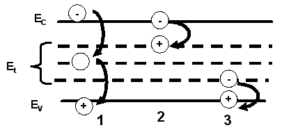
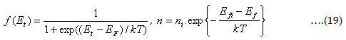
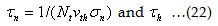
| 4.3.2. Non-radiative recombination (Shockley-Read-Hall process) |
| |
| |
|
| Fig3.11 nonradiative recombination processes (a) recombination center,
(2) electron and (3) hole trap. |
| |
| |
As mentioned before, in this process the electron recombines with hole without any emission,
simply giving away its energy. This non-radiative process competes with the radiative recombination. This usually
takes via surface states or bulk defects and traps, those we are going to discuss now. Generalising the total life
times  (1/Rtotal) (1/Rtotal)
|
|
These nonradiative recombinations are having both positive and negative importance.
For instance, for light emitting applications (such as lasers) nonradiative deactivation is undesirable, whereas
for p-n diodes these are highly essential to increase the speed of device (switching times).
|
Let us consider a trap level (Et) with density of Nt. As you can see, both the
electrons and holes have capture and hole centers at Et.
|
If vth is the thermal velocity (one can derive velocity from 1/2mv2=KBT), n is the electron
concentration and σ is the electron/hole cross-sections ( typically 10-13 to 1015cm2), then the capture rate is given as
|
|
The captured electron from Eq15 will give away energy to phonon with an emission (or capture ) rate of
|
|
 |
Where Pn is the electron emission rate
Similarly the above two equations for holes also exist as
|
|
and
|
|
| at equilibrium Eq15 and 16 are equal similarly Eq17=Eq18. |
| |
| |
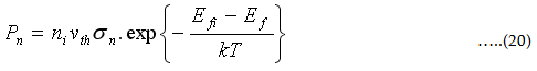
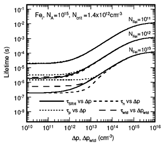
Fig.3.12 SRH life times for different carrier injection with three different dopant levels, in
crystalline Si with Fe as dopant |
We know how to derive the electron density (n) and Fermi distribution (f(Et)) from lecture notes(2) Eq.16 and 20
|
|
one can derive using above expressions the reemitted rate Pn as
|
|
We are interested in the rate of change of carrier concentration (electrons and holes), which is given as
|

|
With little effort one can write Rt in terms of above quantities and defining terms
|
|
|
Above expression is called Shockley-read-hall* equation for recombination rate via
deep levels in the band gap. One can simplify the above expression by assuming
|
|
and Et = Efi
|
|
For low level injection of n-type semiconductor ( n>>p) One would also write above Eq23.
as  , where p and p0 are respectively the non-equilibrium and equilibrium hole electron concentrations
(similarly for holes). Hence the decay rates are not from the majority carriers (here electrons),
but from minority carriers. , where p and p0 are respectively the non-equilibrium and equilibrium hole electron concentrations
(similarly for holes). Hence the decay rates are not from the majority carriers (here electrons),
but from minority carriers.
|
| ---------------------------------------------------------------- |
| ♣ read more at Phys. Rev. B, 67 075203 (2003), and animated simulation software of
SRH available at http://www.imt.fb12.uni-siegen.de/he/aktuelles/srh-e.htm |
| ----------------------------------------------------------------- |
| |
| |
| |
| |
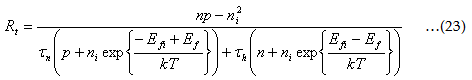
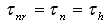
| 4.3.3 Auger♣ Non-radiative processes |
| |
|
| Fig.3.13 Auger recombination representation: (a) 2e-1h and (b)
1e-2h recombination |
| |
| |
As we discussed in the previous section, in the impact ionisation: one hot electron
with energy greater than bang gap scatters another electron into higher states in the valence band to produce two
electron and one hole (similarly for hole). The Auger processes are exactly opposite to this. The schematic
representation of possible electron hole recombination of this kind is given in the fig.3.13. There are two
processes mainly in this recombination:
|
| |
| ----------------------------------------------------------- |
♣ I pronounce it as AUW_gher. There is a hard debate on the pronunciation
of Auger, As it is a French name and is pronounced in France as OZ-Zhey. But many in English speaking people
( though I cant generalize here) pronounce it more like AUW-gher. Some say it is must be the second pronunciation
as it the persons family rout is from German French side. Some also debate it is originated from Anglo-Norman
ancestors of Europe, started as alger
alcher
auger.. ( from Dictionary of British Names 2nd Edition by P. H. Reaney
with corrections by R. M. Wilson © 1976 page 5)
This effect was discovered independently by both Lise Meitner and Pierre Auger in the 1920's. Though the discovery
was made and reported by Meitner in 1923 in the journal Zeitschrift für Physik, two years before Auger discovered the
effect, the English speaking scientific community came to attach Auger's name to it, perhaps because of the political
climate of Europe at the time is marinated with sexism ( comments are not mine!!! comment from www.chemistrydaily.com).
|
| ------------------------------------------------------------- |
| |
| |
| |
(1) one electron from conduction band recombines with hole in valence band
(heavy-hole state) by giving away energy to another electron in conduction band. The energy gained electron jumps
to a higher state and subsequently relaxes to valence band by giving energy as phonon . This is called
conduction-conduction- heavy hole conduction (CCHC) (just after the individual carriers in their respective states)
|
(2) one electron from conduction band recombines with hole in the valence band
(heavy hole state) and knocks one hole deep into the split-off level. This is conduction heavy hole-heavy hole-split
off (CHHS) process.
|
Keep in mind both the processes are non-radiative. The expression for the net Auger
recombination rate is similar to the band-to-band recombination but includes the density of the electrons or holes,
which receive the released energy from the electron-hole recombination.
|
|
Above expression involves both the processes. The non-radiative
lifetimes can simply be written as  . At very high dopant levels, radiative and auger processes
are more dominant. More generalised life time representation is . At very high dopant levels, radiative and auger processes
are more dominant. More generalised life time representation is
|
|
Auger theory is highly dependent on many variants: approximations, band structure
calculations and wave functions.
|
The over all lifetime of recombination is
|
|
More or less the auger processes are not of much importance in wide band gap materials,
as the auger processes here is phonon assisted.
|
| |
| |
| |
| |
| |
| |
| |