| Optical processes in semiconductors |
| |
| |
| 4.2 Optical absorption transitions in semiconductors (e-h pair production): |
| |
| 4.2.1 Band to band transitions |
| |
Any operation related to optical devices clearly depends on the transition of carriers between the
energy levels. The information of optical spectra is highly informative, not only in determining the band gap, but also
in providing characteristic features of the semiconductors (such as direct or indirect), defect levels.
If a wide range of electromagnetic energy is consumed by the valence electron, the excited electrons go to various energy
levels of the conduction band. Besides this, there are also several routes of absorption stages in semiconductors, which we will
discuss later. If we confine our discussion at the moment only to the principal bands, then absorption processes in direct
and indirect band gap are remarkably different. In direct band gap materials, the energy transition is more direct, means
no change in the momentum occurs. Whereas in indirect band gap materials, large change in the momentum occurs, involving either
absorption or emission of a phonon (lattice vibrations). The schematic diagram for direct and indirect band gaps are given in
figure 3.2.
|
| |
| (a) Direct band gap Transitions |
| |
The absorption in direct band gap materials follow the requirement of energy conservation.
If the transition occurs from energies E(k1) to E(k2), where k1 and k2 are initial and final
momentum vectors.
As such, the initial and final energies are written as 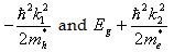 respectively. respectively.
|
| |
|
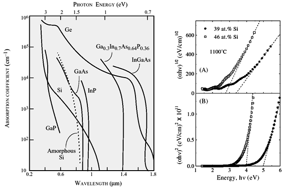
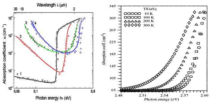
Fig3.3 Absorption spectra of semiconductors ( right) and
indirect and direct optical band gap extraction ( as X axis intercept) from absorption spectra of Silicon |
| |
(Here Eg is the direct band gap at k=0 and the absorbed photon energy is
Ephoton= E(k2)-E(k1), which is energy conservation requirement. Also note that m*h and m*e are respectively the
effective masses of holes and electrons in the valence and the conduction band)
|
| |
The transition probability for the energies E(k1) to E(k2) can be calculated from first
order time dependent perturbation theory.
Without going into the details, the transition probability (per unit volume and per unit time) for direct transition is ,
|
|
| |
where 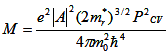 and mr*=(1/me*+1/mh*) and P2CV is the matrix
element of momentum operator and A is the magnetic vector potential . Eq1 contains the reduced density of states given by and mr*=(1/me*+1/mh*) and P2CV is the matrix
element of momentum operator and A is the magnetic vector potential . Eq1 contains the reduced density of states given by
|
|
In reality, we will see the consumption of photon from the given electromagnetic energy.
Thus, it is important to see how we can relate the ratio between the incident photon intensity (I0) and the absorbed
photons intensity (I). In steady state and in a direction normal to the incident light, I/I0=exp(- αd), where α is the
absorption coefficient and d is the thickness of the sample. From Eq. 1 and incorporating the radiation energy cross
section, we can write the absorption coefficient as
|
|
The above equation can be simply written as 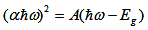 for direct bandgap semiconductors. It suggests that from absorption
(absorption, A=αd) spectra it is possible to estimate the direct band gap. However, in many practical cases, the above linear relation is
dominant only for some region and the possibility of additional transitions coming into the absorption will be discussed later in detail. for direct bandgap semiconductors. It suggests that from absorption
(absorption, A=αd) spectra it is possible to estimate the direct band gap. However, in many practical cases, the above linear relation is
dominant only for some region and the possibility of additional transitions coming into the absorption will be discussed later in detail.
|
| |
| |
| (b) Indirect band gap transitions |
| |
As mentioned before, the electron photon interactions in indirect band gap are assisted by phonons (Fig3.2b).
So, the conservation of momentum and energy
|
|
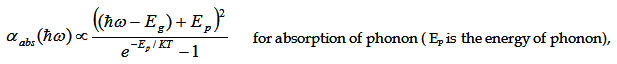
Here we have two cases- generated from phonon absorption and emission. In the emission of phonon, the energy of the
absorbed photon could be equal to the direct band gap or at least close to k=0. Finally, the electron moves from this state to indirect band
gap by phonon scattering. The level where the electron waits for phonon assistance is a virtual state.
The transition probabilities involving these virtual states could be solved by second order perturbation theory. But keep in mind that
the initial and final states of electron transition involve the energy range from the product (and/or difference) of photon and phonon
energies. Hence, the total probability is the sum of all the states.
The absorption coefficient of transition with phonon involvement
|
|
and
|
|
The above transition equations, obviously, hold when the photon energy is greater
than Eg-Ep and Eg+Ep respectively.
|
|
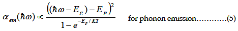
| Fig3.4 Absorption edge of (a) a direct band gap semiconductor and (b) indirect band gap semiconductor.
The energy Evert marks the threshold for the vertical transition. |
Since the photon energy could be higher than the sum of band gap and the phonon energies, the total α is the
numerical sum of both phonon absorption and emission absorption coefficients.
|
It is very nice to compare (Eq4 and Eq3) in the band gap evaluation for both direct and indirect band
gap semiconductors from optical absorption spectra. The former relation is 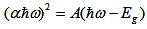 whereas here it is whereas here it is  , where Eth involves phonons.
In practice, the band gaps evaluated from the optical absorption are referred as optical band gaps. One also has to keep in
mind that, in indirect band gap, there is a high possibility of wrong estimation, as earlier we considered scattering through
phonons only, whereas here we have to consider scattering due to impurities also. Schematic representation of absorption band
gaps in both the semiconductors is shown in figure 3.4. , where Eth involves phonons.
In practice, the band gaps evaluated from the optical absorption are referred as optical band gaps. One also has to keep in
mind that, in indirect band gap, there is a high possibility of wrong estimation, as earlier we considered scattering through
phonons only, whereas here we have to consider scattering due to impurities also. Schematic representation of absorption band
gaps in both the semiconductors is shown in figure 3.4.
|
| |
| |
| |
| 4.2.2 Intra band transitions |
| |
| |
| |
| (a) Donor acceptor related absorptions: |
| |
| |
Although it is theoretically approved, at least quantitatively, that if we know the density of states
and the carrier contribution, we can derive the absorption coefficients as a function of the energy. However, we should not
forget that the density of states at conduction band and valence band are not having abrupt ends to create a band gap, but
there is always a band tail creeping into the band gap region. An Ionized donor exerts an attractive force on the conduction
electrons and a repulsive force on the valence holes (acceptor act conversely). Since impurities are distributed randomly in
the host crystal, the local interaction will be more or less strong depending on the local crowding of impurities. The possible
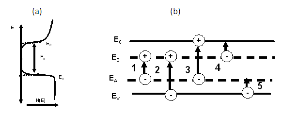
transitions of donor acceptor levels are illustrated in the figure 3.5.
|
|
| Fig.3.5 Schematic representations of band tail in direct band gap semiconductors
(b) donor and acceptor related various transitions. |
| |
As you have seen in your previous lesions, the deep impurity states move up and down with the potential
of the associated band edge (acceptors move with the valence band edge). Hence, at high concentrations, the impure states form a
band whose distribution creeps into the energy gap like an associated band edge. These are called deep levels. The transitions either
between two impurity levels (transition 1 from Fig 3.5b) or between the impurity level of the conduction/valence bands
(transition 2 and 3) are called deep level transitions. Hence, the absorption coefficients of these transitions are highly
dependent on the doping levels.
For better device performance of direct band gap semiconductors, the deep level defects should be avoided as much as possible.
The reason is that these levels act as trap centers for electron and as a consequence, they can not participate in current flow.
However, in the case of indirect gap semiconductors, these defect levels are purposely introduced to increase the optical response
of the material. This is done primarily to increase the
|
| |
|
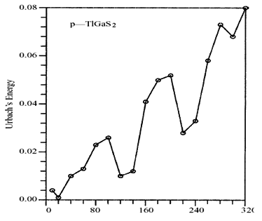
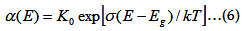
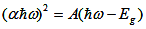
Fig.3.6 Absorption spectra of n-InSb with different dopant levels (T=130K) (B) temperature
variation of p- type TlGaS2 absorption and (C) Variation of Urbach tails with temperature
|
probability of transition with the aid of these deep levels, as they have all the possible k values present.
The transition between the band tails leads to an exponentially increasing absorption coefficient
(as d(lnα)/d(E)=1/kT) and is known as an Urbachs rule.
It suggest that the absorption tail is strongly dependent on temperature. (Why it should be? Is there any
relation between temperature and donor/acceptor probabilities? Explore your self).
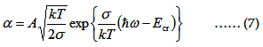
Absorption coefficient for Urbach tails could be written as
|
|
(K0 and A are constants , and σ represents the scaling factor for sharpness of the edge.)
|
On comparing this equation with the Eq1 for direct band gap
 , ,
If we look at the total energy continuity, (both the edge and tail existence), we will see a crossover of
critical energy 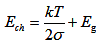 (try to prove this relation yourself !) (try to prove this relation yourself !)
|
Hence the absorption spectrum reveals that for photon energies above Ech, the behavior
follows direct band gap (Eq1) and below Ech it follows the Urbachs rule ,
|
|
For experimental convenience it is simply written as,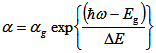 , where ΔE is the Urbach tail
and Eg and αg are optical band gap and absorption coefficient respectively (at Eg). , where ΔE is the Urbach tail
and Eg and αg are optical band gap and absorption coefficient respectively (at Eg).
|
| |
| |
| (b) Exciton absorption |
| |
These transitions are most exceptional transitions. These transitions appear only in
|
|
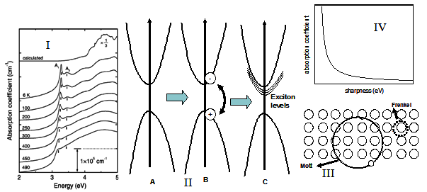
| Fig. 3.7 (I) temperature variation of exciton spectra of wide gap oxysulphide semiconductor
(APL 2001), (II) exciton formation and (III) mott and Frenkel excitons (IV) |
purest semiconductors. The pairing of electron hole pair produced near the band gap is called exciton*.
This exceptional pairing behaves like as if they are electron-proton pair in a hydrogen atom with a definite binding energy. We can
understand this concept with the help of a simple schematic of band structures given in Fig 3.7(II). In figure A, we show the full
valence band and empty conduction band. Under these conditions, there are no allowed states within the gap. Here we are talking about
pure semiconductor; hence, there are no donor-acceptor levels. Now consider a case where there is one electron in the conduction band
and one hole in the valence band (II). This new situation has changed the electronic system. We now have an additional Coulombic interaction
between the electron and the hole. The electronic band structure should thus be modified to reflect this change resulting in additional
exciton states below the conduction band (III). The excitons (the quantized electron pair) appear in pure semiconductors** because of their
low binding energies and they are strongly temperature dependent. As you see from the experimental result, Fig3.7 (I), exciton peaks appear
at very low temperature with enormous absorption coefficients and narrow line widths. Such narrow peaks show innumerable applications in
optoelectronic devices such as lasers and in quantum electrodynamics. These excitons are further enhanced in quantum well semiconductors.
Exciting details of these excitons, you will learn from your optoelectronics lectures, if you have any.
|
| -------------------------------------------------- |
* Find more information on another type of quantized quantity, namely, polaritons. Polaritons are the
quasi particles born from the strong interaction of excitons with photons in highly confined geometries of semiconductors.
** Is it really true that the excitons appear only in pure semiconductors? Prove it by searching for impure semiconductor excitons!!
|
| |
|
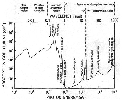
Fig.3.8 Different types of optical absorption phenomena; (1) transitions of high-lying bands, (2) excitons, (3)
fundamental absorption (valence-band-to-conduction-band transition and Urbach-tail), (4) impurity absorption, (5) free-carrier absorption
|
| |
Briefly, the absorption coefficients are related to the sharpness of the exciton peaks. The absorption coefficient
equation for exciton transition is very similar to the direct band gap equation (Eq.8),
|
|
where σ is width of the exciton peak, aex is exciton radius
( typically  100A for most of the semiconductors)
and remaining terms stand as explained in previous sections. Eq.8 suggests that the absorption coefficients exponentially
increase with the sharpness of the exciton peak ( Fig 3.7 IV). There are two important classes of excitons one would expect
depending on the spatial extent of the periodic envelope function ( which is a function of exciton radius). When it is confined
to just few unit cells, the excitons are classified as Frenkel excitons. On the other hand, if the envelope function extends
to several hundreds of Angstroms, then such excitons are called Mott excitons. Mott excitons are mostly responsible
for total excitonic optoelectronics of semiconductors. Figure 3.7 III shows schematically both assuming open
circles are unit cells*. 100A for most of the semiconductors)
and remaining terms stand as explained in previous sections. Eq.8 suggests that the absorption coefficients exponentially
increase with the sharpness of the exciton peak ( Fig 3.7 IV). There are two important classes of excitons one would expect
depending on the spatial extent of the periodic envelope function ( which is a function of exciton radius). When it is confined
to just few unit cells, the excitons are classified as Frenkel excitons. On the other hand, if the envelope function extends
to several hundreds of Angstroms, then such excitons are called Mott excitons. Mott excitons are mostly responsible
for total excitonic optoelectronics of semiconductors. Figure 3.7 III shows schematically both assuming open
circles are unit cells*. |
| |
| |
| (c) Free carrier absorption |
| |
As the name suggests, the mechanism of the absorption involves the photon absorption of a free carrier within a
band and as a consequence that free carrier is raised to the higher levels. This transition is within the valley and must conserve
momentum. To obey the conservation of momentum, it must be assisted by the impurity scattering and lattice vibrations (phonons).
These transitions are within a band only, hence these will appear at very low energy regions of the spectrum.
Free carrier absorption is quite different for electrons and for holes, mainly due to the presence of multiple valence bands.
In the case of n-type semiconductors, conduction band electrons are only excited by photon and phonon, in order to conserve
momentum. By contrast, p-type semiconductors can have direct (i.e. no phonon needed) transitions between the heavy and light
hole bands in the valence band. As such in p- type, carrier absorption is much stronger than n-type.
The absorption coefficients of free-carriers is related to wavelength of electromagnetic
spectrum by α( ω) ∝ λp , ( p ranging from 1.5 to 3.5). Hence there is a monotonic increase in the free carrier
absorption spectrum (Fig3.8).
|
| |
| ----------------------------------------------------------------- |
♣ see the article Physics News 277, July 1, 1996 talking about AN EXCITON ANALOG OF A LASER
( it is almost 10 years back story, now many researchers realized a laser out of it)
may be possible, in a semiconductor
crystal, an electron can be excited from a valence state to a conduction state.
Another nearby electron can fill the hole left behind, but this only moves the hole to a new location. In effect,
the hole acts like a positively charged object which can move about and bind itself to a negatively-charged electron.
This tiny "atom" is called an exciton. Under special conditions excitons can condense into clouds. Insofar as excitons
are bosons (particles with a spin of 0 or 1), they can even coalesce into a single quantum state, namely a Bose-Einstein condensate.
Physicists at the University of Ottawa (Emery Fortin, fortin@physics.uottawa.ca) and the Ecole Polytechnique in Palaiseau,
France have shown that it is possible to amplify a coherent beam of energy based not on light waves, as in a laser,
but on excitons. In their experiment a laser creates an ongoing bath of excitons in a small semiconductor sample.
A second laser establishes a small moving cloud of excitons (350-400 microns in size). Through a process of stimulated
scattering the moving cloud gains new excitons as it proceeds; it grows not in size but in density. In other words,
the directed beam of excitons is undergoing amplification. Because "exciton mirrors" do not yet exist, this
amplification process occurs only over a single pass through the sample, and consequently there is not the repeated
buildup of signal one gets in a laser. Furthermore, because excitons subsist of electrons and holes in the crystal,
a beam of excitons could never be extracted from the sample and exist as an external beam as laser beams do. Still,
the exciton beam in this present experiment may offer new ways of studying the coherent transfer of energy and charge.
|
| Finally, we can conclude that the absorption of semiconductor uniquely represents the characteristic features of material. |
| |
| |
| |
| |
| |
| |
| |
| |
| |
| |
| |
| |
| |