| Optical processes in semiconductors |
| |
| |
| 4.1 Introduction |
| |
In Chapter 2, we learnt how an electron behaves in a crystal lattice. Various
interesting properties of semiconductors such as energy band formation, mechanisms of electron scattering and finally
the electron transport were clearly discussed in the previous chapter. However, we have not seen how an electron, having
gained energy from external means, gets transported to higher energies. When one electron leaving the energy level
creates a hole, the process is called electron-hole pair generation. Similarly, when an electron combines with the hole,
the process is called recombination. In this chapter, we examine various possibilities of electron-hole pair generation
and also examine recombination mechanisms. This electron-hole pair generation and recombination process is very
important in device technology, particularly in optoelectronic devices. This concept is the basis for the working
principle of an LED (light emitting diode) and semiconductor laser. Though we have generalised as optical processes,
we will also see how these processes influence other processes such as electrical properties of a device
(such as p-n diodes). In this chapter, we will review e-h processes involved in semiconductors and some of the
intrinsic properties.
|
Creation and recombination of e-h pair essentially require external energies such
as optical, electrical or thermal energies. Such processes are mainly between the valence band and the conduction band.
General concept is the pair production (or recombination) within the volume, and hence, although the local carrier
concentration changes, overall space charge remain neutral. We can categorise the e-h pair channels into three
categories: radiative, nonradiative and thermal processes. Here we have to consider several time-scales, energy
bands and charge carrier concentrations of particles at the specified energy levels.
Before going deep into it, let us review few transitions that you learned in your previous classes related to optics.
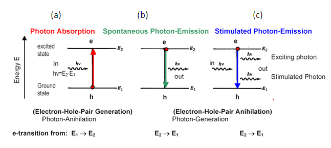
If we give sufficient energy (energy equal to band gap), one electron raises from the valence band to the conduction
band, leaving a hole in the valence band. This is called absorption. Once the electron reaches
conduction band, it simply comes down and recombines with the hole (stay time depends on the energy level life time).
This recombination energy must be consumed and may get converted as a photon (luminescence) or given away to the
lattice as phonon or heat. The energy conversion of photon is called radiative transition and conversion
to phonon or heat energy is called nonradiative transition.
|
| |
| |
Radiative pair recombination (emission, also called luminescence) event takes
place by emitting a photon whose energy depends on the kinetic energy gained and the band gap of the material.
This process could be either stimulated (by population inversion) or just spontaneous. However, in reality, the
nonradiative processes greatly influence the radiative and also band-to-band transition processes.
|
| |
For simplicity and for the time being, we designate band states as conduction
and valence band (keep in view the picture of direct and indirect band gaps) and the bound states are the impurity
levels, phonon or imperfections in the semiconductors. The bound states, unlike donor and acceptor states, they do not
really ionize, but act like traps or more like short time home for either electrons or holes.
|
| |
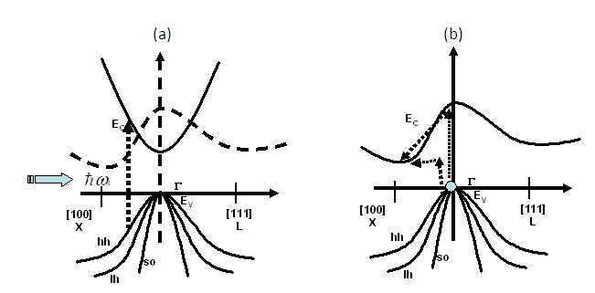
Optical processes directly involve photon absorption and emission.
This process is clearer in direct band gap materials such as GaAs, where conduction minimum and valence band
maximum lie at the zone center (k=0). Hence it is easy for an electron to rise to the conduction band by absorbing
a photon of energy equal to the band gap Eg, and come down to the valence band and recombine with a hole by liberating
the energy as emitting photons. As such, the probability for radiative process in direct band gap materials is very high.
Whereas in indirect band gap material, such as Silicon, the process requires additional momentum or the involvement of phonon,
as the conduction and valence band centers do no match at k=0. In such cases, phonon emission or absorption can assist
the e-h recombination. As such, electron takes a long time, waiting for such a phonon event to occur, at the conduction
level. As we talked before there are defects traps those acts as recombination centers or just a springboard. It is highly
likely event that the e-h combination is nonradiative and the excess of energy is dissipated as lattice heating.
In other words, in indirect band gap nonradiative processes dominate. Hence, these devices are considered ineffective
as emitting devices. (Not for so long: The recent discovery of converting Silicon as an efficient emitter, in reduced
dimensions of silicon, made such assumption obsolete. We shall discuss this in our spare time).
|
| |
| |
|
Fig.3.1 (a) Showing absorption of photon when light of
sufficient energy is incident (b) Photon Emission in the absence of external photons (c) Photon emission in the presence
of external photon |
| |
Another important channel of nonradiative process involves deep levels of either
conduction or valence bands. Here the process involves a third free carrier, which is eventually raised to higher energy
levels via intra band transitions. This comparatively high energy related process is very important in heavily doped
semiconductors and is called Auger recombination process.
|
| |
|
Fig.3.2 Absorption process in (a) direct and (b) indirect band gap |
| |
As we discussed before, the e-h pair production or recombination involves either
band to band or intra band transitions. Let us see how we can export an electron from the valence band to conduction and later
we will explore various possibilities of the electron recombination with the leftover hole.
|
| |
| |
| |
| |
| |
| |
| |
| |