| Fundamental concepts of semiconductors |
| |
| |
| |
| |
| |
| 3.2 Macroscopic Transport |
Till now we have studied about the carrier densities of electrons (or holes)
and the physical picture of energy levels. Now we shall apply our basics to understand the carrier transport in
semiconductor, which is an essential phenomenon in semiconductor devices.
|
|
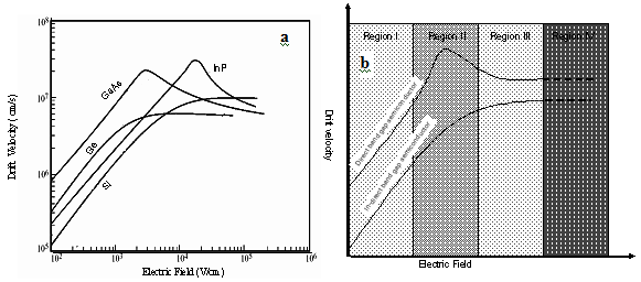
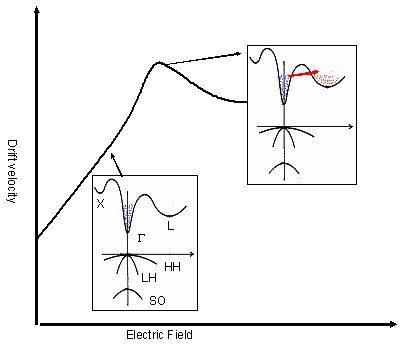
Fig2.41: (a) Drift velocity -Electric field response of semiconductors
at 300K. (b) Schematic representation of region-wise velocity-field response (I) low field (II) High Field (III) saturation
and (IV) impact-ionisation region
|
|
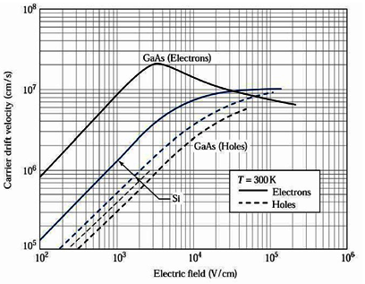
Fig 2.41 (c) Variation of
drift velocity of carriers ( electrons and holes) with electric field for a direct (GaAs) and an indirect (Si) band gap
semiconductor. Why drift velocity changes from electrons to holes?
|
Let us generalize that the free carrier motion of any type in a semiconductor leads to a current. Such motion can be driven by external electric field, since the carriers are charged particles. We will refer to this transport mechanism as carrier drift. In addition, carriers can also move from regions with high carrier density to much lower carrier density regions, similar to liquid flow. This carrier transport mechanism is due to the thermal energy and associated with random motion of the carriers. We will refer to this transport mechanism as carrier diffusion. Hence, the majority of the current in a semiconductor equals the sum of the drift and the diffusion current.
Figure 2.41 represents the drift velocity response of some important direct and indirect semiconductors, under the influence of electric field. As you can see from the figure, the drift of the carriers is markedly different from direct band gap materials to indirect band gap materials and the behavior is quite complex. However, we can qualitatively explain this behavior by dividing the total region to low, high and very high field regions.
|
| |
| |
| |
| |
| 3.2.1 Carrier transport by Drift -Low Field ( Linear region) |
Where the drift velocity is directly proportional the Electric field and both carriers
and lattice atoms are at equilibrium. This is same for both direct as well as indirect band gap materials. Here the drift
velocity is 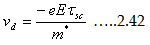 strongly dependent on various scatterings such as lattice and impurities) and also effective mass. strongly dependent on various scatterings such as lattice and impurities) and also effective mass.
|
| |
|
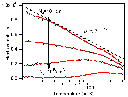
Fig. 2.42 Electron mobility variation with temperature in n-Ge for various
concentrations of dopant. Here you observe the impact of lattice ( T-3/2 ) and impurity (T3/2) Scattering dependence.
|
| |
| |
| |
| |
| 3.2.2 Carrier transport by Drift- High Field |
In high fields (typically up to 100kVcm-1), electron get more thermal energy and the
temperatures go much higher than the lattice temperatures. The linear relationship between the average carrier velocity
and the applied field breaks down when high fields are applied. As the electric field is increased, the average carrier
velocity and the average carrier energy are also increased. The description of carriers, however, is quite complex and
difficult to realize with simple numerical equations. But it is possible to summarize the behavior of carriers broadly
for both direct and indirect band gap materials.
|
|
Fig.2.43.Schematic representation of inter-valley transfer in direct band gap materials
|
| |
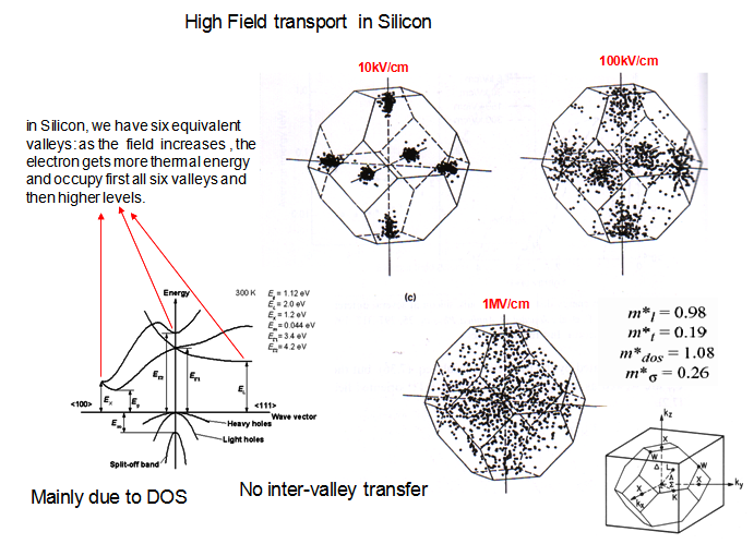
For the carriers in indirect band gap materials such as silicon, which do not contain accessible higher bands, the velocity versus field relation increases monotonically as shown in Fig2.44. Specifically for silicon, where it contains six equivalent energy valleys: as the field increases, the electron gets more thermal energy and occupies higher levels. ( For Si, there are six equivalent points
(2 π/a)(0.85,0,0),
(2 π/a)(0,0.85,0), (2 π/a)(0,0,0.85) and inverse of these three). The monotonic increase (two orders of magnitude) and saturation of velocity is similar in all indirect band gap materials (see figure 2.44).
|
|
| Fig 2.44 Schematic representation of high-field effects in indirect bandgap semiconductors, example for Silicon is giving here. Unlike direct band gap Silicon is having six-equivalent energy valleys (2 π/a)(0.85,0,0); (2 π/a)(0,0.85,0), (2 π/a)(0,0,0.85); And inverse of these three). Therefore as the field increases , the electron gets more thermal energy and occupy first all six valleys simultaneously and then higher levels. The schematic representation of valley filling at Electric fields is schematically shown. We can call this transport as “intra-valley” transfer. |
| |
| |
| |
| Whereas in the direct band gap materials it is entirely different, because, they contain multiple closely spaced conduction minima (for example, in GaAs, EΓ=1.42eV; EL=1.71eV; Ex=1.90eV) for electron transport.
Typically, the variation in the mobility is due to the inter valley transfer from the zone center valley
(EΓ; m*=0.067m0) to L (EL; m*=0.22m0)
valley having different effective mass contributions. Below a certain field, electrons are primarily in low effective
mass and a high mobility valley that is Γ valley. As the field is increased, the electrons get transferred from
the totally filled Γ valley to slightly higher L valley, where the difference between these two valleys is
~0.3eV.
This is called Inter-valley transfer (see fig.2.42). Schematic representation of inter-valley
transfer is given in the figure. Since upper valley electrons are heavy, the electron velocity decreases even
though the field is increasing. This type of field behavior is desirable for some specific devices such as
high-frequency microwave devices. For instance, low mass and high inter-valley separation is needed to
have superior velocity-field behavior, for instance a material In0.53Ga0.47As (m*=0.04m0 and Γ-L separation= 0.55eV)
shows higher peak velocity than conventional GaAs. |
| |
| |
| |
| |
| 3.2.3 Carrier transport by Drift- Very High Field ( Breakdown) |
| |
|
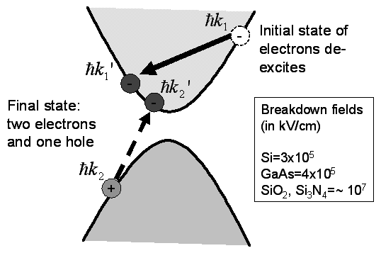
Fig2.44: Impact ionisation process in semiconductors. Carrier multiplication
is due to one very hot electron knocks out electron from valance band, creating two electrons and one hole at the final stage.
|
| |
In the previous sections, it was mentioned that electrons (or holes) stay
in their respective bands only. But at extremely high fields (typically >100kV/cm) this is not true. If the
energy supplied by the external field exceeds the band gap energy, very hot electrons in the conduction band
knock out one electron from the valence band to the conduction band. Finally, we end up with two electrons and one hole!
(but, remember, the total number of electrons is always conserved). Schematic representation is as shown in the figure
2.45. This breakdown, rapidly increases the carrier multiplication rate and the process is called impact
ionization or avalanche process. This process can be defined by
 where I is the current and αt
is the average rate of impact ionization per unit time. The critical breakdown
field is defined where αt approaches 104cm-1.
Breakdown fields of some of the important materials, that are useful in devices, are given in the figure
2.45. This process, keeps an important limitation to the devices, where due to carrier multiplication,
control over device is completely lost. However, in particular devices such as photo-detectors, this
behavior is very useful to achieve high-gain detection. We will revisit this process again in subsequent
chapters, when we are dealing with the applications. Thus, it is very critical to design a semiconductor
(what we say is band gap engineering) in such a way that it sustains as very high power devices. where I is the current and αt
is the average rate of impact ionization per unit time. The critical breakdown
field is defined where αt approaches 104cm-1.
Breakdown fields of some of the important materials, that are useful in devices, are given in the figure
2.45. This process, keeps an important limitation to the devices, where due to carrier multiplication,
control over device is completely lost. However, in particular devices such as photo-detectors, this
behavior is very useful to achieve high-gain detection. We will revisit this process again in subsequent
chapters, when we are dealing with the applications. Thus, it is very critical to design a semiconductor
(what we say is band gap engineering) in such a way that it sustains as very high power devices.
|
Briefly, about mobility of carriers:
Assumptions we made so far for low field:
|
- Electrons suffer collisions from many sources and scattering mean time
 gives the mean time between successive collisions. gives the mean time between successive collisions.
- Electrons do not interact with each other.
- Scattering processes: dominantly electron-electron and electron-phonon interactions
- The average drift velocity with effective mass m* traveling in the field F is

- Comparing with Ohm's law, the conductivity

- From the definition of velocity and Field, mobility
 ( for holes and electrons the mobility is different as the
effective mass is varying, similarly conductivity rewriting for both electron and hole, ( for holes and electrons the mobility is different as the
effective mass is varying, similarly conductivity rewriting for both electron and hole, 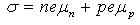 ) )
|
| |
| |
|
(i) Low field effects:
|
- Under band gap transitions
- Conduction is proportional to the applied field ( in all semiconductors)
|
|
|
(ii) High field effects:
|
- Band-to-band transitions
- Conduction in direct band gap Semiconductors ( such as GaAs) : inter-valley transfer
- Conduction in indirect band gap Semiconductors ( such as Si): Equal distribution among the low lying all six valleys
|
|
(iii) Very High Field Effects:
|
- Carrier multiplication; production of additional carriers due to interaction of very hot carriers.
|
| |
| |
| |
| |
| |
| |
| |
| |
| |
| |
| |