| Fundamental concepts of semiconductors |
| |
| |
| |
| |
| |
| 3.1 Scattering Phenomena |
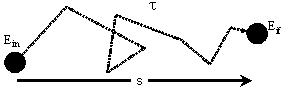
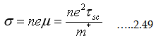
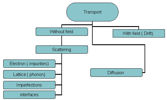
So far, we have learned about the energy band structure and the carrier densities of semiconductors. Such knowledge is very important to understand the dynamics of electrons in semiconductors while they experience external fields such as electrical and optical fields. In a very general fashion, we can define the flow of electrons and/or holes in semiconductor as transport or current. As we came to know from our previous sections that, when electron leaves the bound states, it creates a hole which is called electron-hole pair generation and similarly when electron returns by consuming the hole position, the process is called electron-hole pair recombination. When we are talking about the electric field response of semiconductor two aspects must be considered: (1) electron drift as well as diffusion transport and (2) electron-hole pair generation and recombination. Both these are considered separately. Total transport is defined by the summation of drift, diffusion and carrier generation and recombination, as schematically represented in fig 2.34. Key questions we are going to address are
|
- When there is no electric field is there any transport?
- How does the electrons and holes transport under electric field influence?
- Is there any effect of concentration gradient of carriers on transport?
- Do the electrons simply fall down to valance band or is there any significance in the total conduction?
|
 |
| |
Let us start when there is no electric field.
|
In general, if you apply an electric field (F) to a perfect semiconductor, the electrons behave more like free space electrons governed by an equation of motion,  .
An electron in the k-space constantly gain and lose momentum and do the oscillatory motion. Such oscillations are
called Bloch oscillations. However, these oscillations occur at very low temperatures or in very special
semiconductor designs In real systems, electrons (or holes) experience, scattering due to (1) impurities, (2)
lattice and (3) imperfections on the surfaces (or lattice mismatch) which affect the transport of carriers.
For our discussion, let us restrict ourself to most significant scatterings, lattice and impurities.
As shown in the figure one can consider an electron, moving with a certain energy and momentum. Due to
the scattering processes, both energy and momentum gradually lose coherence with the initial state
and reach to new final values. The average time it takes to lose coherence of the initial state is
called relaxation time or scattering .
An electron in the k-space constantly gain and lose momentum and do the oscillatory motion. Such oscillations are
called Bloch oscillations. However, these oscillations occur at very low temperatures or in very special
semiconductor designs In real systems, electrons (or holes) experience, scattering due to (1) impurities, (2)
lattice and (3) imperfections on the surfaces (or lattice mismatch) which affect the transport of carriers.
For our discussion, let us restrict ourself to most significant scatterings, lattice and impurities.
As shown in the figure one can consider an electron, moving with a certain energy and momentum. Due to
the scattering processes, both energy and momentum gradually lose coherence with the initial state
and reach to new final values. The average time it takes to lose coherence of the initial state is
called relaxation time or scattering  time. The scattering time from
all above possible sources such as impurities etc.,
result into to the total scattering time, time. The scattering time from
all above possible sources such as impurities etc.,
result into to the total scattering time, 
|
| |
| |
| At low fields, the macroscopic transport property of the material (such as conductivity) can be related to the microscopic properties such as scattering times. |
|
Fig.2.35 Schematic representation of scattering of electron |
| |
Assuming that the carriers in semiconductor do not interact with each other and after each successive collisions
with the scattering centers, reaches to the final position.
The average velocity gain, in between the collisions, that is only for the time , can be given as
|
|
| |
Where m* is the mass of the carrier and  is called drift velocity. But from the
definition of mobility, the drift velocity is proportional to the electric field, is called drift velocity. But from the
definition of mobility, the drift velocity is proportional to the electric field,
|
|
| |
(Note that the electrons move in a direction opposite to electric fields and holes in the direction along the field)
From the both equations we can define mobility as
|
|
Therefore, it is clear that the mobility is dependent on scattering mechanism and effective mass.
But how it is related to conductivity? We know that the current density is
|
|
| |
and according to ohms law the current density is
|
|
| |
Combining all we get conductivity expression as
|
|
|
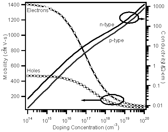
Fig.2.36 Effect of doping concentration on mobility (of electrons and holes )
and conductivity of silicon.
|
If we write electrons mobility as μn and for holes μp, the total conductivity can be written as
|
|
Quick note: mobility is high if effective mass is low and loss, scattering implies large
scattering and therefore high mobility.
To understand the macroscopic transport more, let us look into the discussion to most significant scatterings, lattice and impurities.
|
| |
| |
| |
| |
| 3.1.1 Electron-Phonon Scattering or Lattice Scattering: |
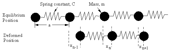
As we learned earlier, a crystalline lattice is a collection of different masses and arranged in a particular geometry. The atoms in a crystal are tightly bonded with each other by electron bonding. Elastic forces, with some minimum potential energy, hold these bonds together. As a consequence, the system (strictly speaking, the atoms) will be under oscillations about its equilibrium position. These oscillations could be either longitudinal or transverse waves. (We can imagine an artificial system where atoms are linked to mechanical springs, is seeing the situation now). These vibrations are called lattice vibrations and the quanta of such vibrations are phonons.
|
|
Fig 2.37.Atoms ( of equal masses m) linked to the mechanical springs
|
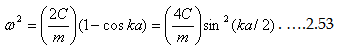
Assume a crystal as one dimensional (diatomic molecule lattice)
containing
two atoms
having equal mass m. If we solve the force equations for 2n and 2n+1 atoms, using
|
|
and according to Newtons force equation
|
|
Where the displacement un = u exp(i( ωt-2nka)) , u is amplitude, k is the wave
vector with a as spacing between the planes.
After solving both we arrive at the dispersion relation between ω and k as
|
|
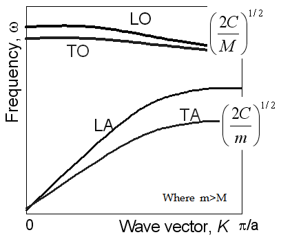
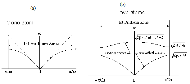
Fig.2.38 Dispersion relation for (a) mono atom (b) two atoms in 1D.
|
| |
|
It is interesting to observe the above relation at boundary condition  , that is
exactly our Brillouin zone (BZ) boundaries;
We observe that the frequency attains the maximum at BZ boundaries, as shown in the figure 2.38. , that is
exactly our Brillouin zone (BZ) boundaries;
We observe that the frequency attains the maximum at BZ boundaries, as shown in the figure 2.38.
|
| |
If we extend the same argument for two diverse atoms (of mass m and M) we get quadratic equation containing ω and the solution is
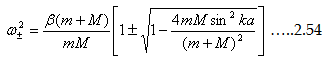
representing optical and acoustic phonon vibrations respectively. This relation appears simple in diatomic systems, whereas in complex systems it is much more complex.
Let us think how optical and acoustic phonons are different. For optical branch, two atoms move opposite to each other, while in acoustic branch, both the atoms movie with the same amplitude, phase and direction. Also, each optical and acoustic branch has two modes: two transverse and two longitudinal modes for Acoustic and optical branches, and they denoted TA & LA and TO & LO.
|
Fig.2.39.Dispersion relation for system of two atoms of different mass. |
| |
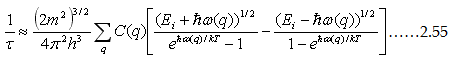
The electron phonon coupling strengths C(q) are related to scattering times as
|
|
| |
Generalizing above discussion, acoustic vibrations are due to atoms in a basis
cell vibrating with the same sign, whereas optical branch is due to the atom that vibrates with opposite sign.
Theoretical calculations reveal that the mobility in non-polar semiconductors, such as silicon and germanium,
is dominated by acoustic phonon interaction. The resulting mobility is expected to be proportional to (m*⁄T)3⁄2 , while
the mobility due to optical phonon scattering only is expected to be proportional to T-1/2 .
|
|
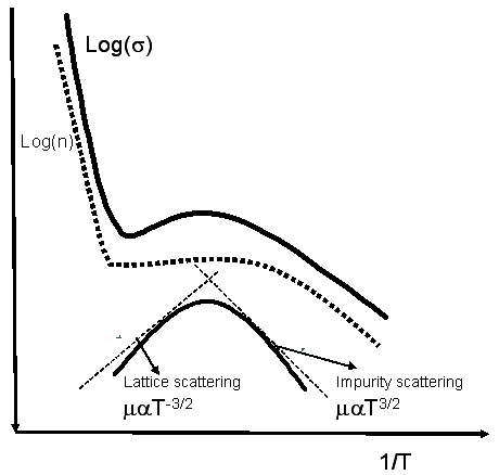
Fig2.40: Schematic representation of effect of lattice and impurity scatterings
on conductivity in extrinsic semiconductors. Observe that the scattering takes place in the region of operating temperatures.
|
| |
| |
| |
| |
| 3.1.2 Impurity Scattering or electron-electron scattering: |
Impurities are foreign atoms in the solid, which are efficient scattering centers, especially
when they have a net charge. Ionized donors and acceptors in a semiconductor are a common example of such impurities.
The amount of scattering due to electrostatic forces between the carrier and the ionized impurity depends on the interaction
time and the number of impurities. Without going into further details, the mobility due to impurity scattering is proportional
to T 3/2⁄NI, where NI is the density of charge impurities. Effect of lattice and impurity scatterings on conductivity in
extrinsic semiconductor is shown in fig. 2.40
|
| |
| |
| |
| |
| |
| |
| |
| |
| |