| Fundamental concepts of semiconductors |
| |
| |
| |
| |
| 2.2 Extrinsic semiconductors |
| |
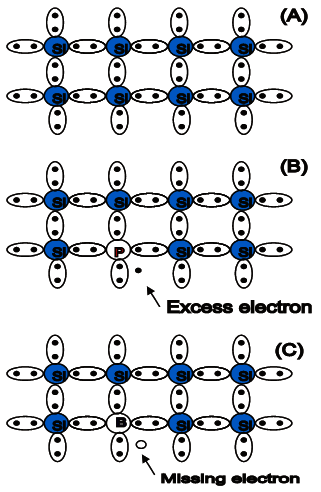
Pure ( intrinsic ) semiconductors may be of interest for many applications but the addition of impurities in controlled amounts of Impurity would take semiconductor performance into new dimensions. Let us take our well-known silicon as an example. From our previous discussions we came to know that silicon is covalently bonded with four silicon atoms (Fig 2.27). It suggests that there are no free electrons available for external meddling. Adding a small amount of (how much?) electrons (or holes) would dramatically change the conducting properties of Silicon. Effect of doping (addition of either electron acceptors or electron donors) will increase the densities of respective carriers and hence the change in the conductivity. However, the atomic dimensions of the impurities should be typical of the dimensions of the intrinsic semiconductor atoms. Depending on the dopant, electrons or holes, the semiconductor may be an N-type or P-type. (The prerequisite for a dopant is that they must contain an excess of electrons (or holes). ) Let us look at n-type and p-type doping in semiconductors.
|
| |
| |
| 2.2.1 n-type doping |
| |
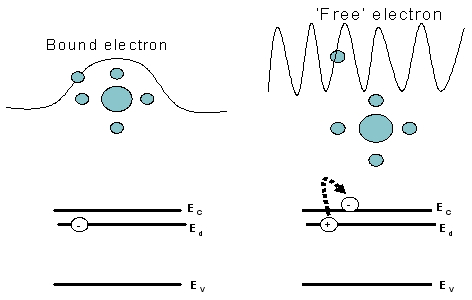
Group V elements in the periodic table are, in general, considered for n-type doping. Typically, Phosphorous, Arsenic and Antimony are the elements from group V. They have five electrons in the outermost shell and if it replaces an intrinsic silicon atom, one electron will remain as excess. Such kind of elements is called Donors (see figure 2.27(B)). Thought, the impurity atom is strongly bonded into the crystalline structure by replacing one semiconductor atom, this excess (additional) electron is loosely bounded, and therefore it behaves more like a free-electron. In the band diagram, the energy levels of these donor atoms lie in the forbidden gap, slightly below the conduction band of intrinsic semiconductor.
|
| |
Table 2.2.1 |
| N-type dopant |
P-type dopant |
| Called Donors |
Called Acceptors |
| Group V impurities (e.g. Antimony, Phosphorous, Arsenic etc., ) |
Group III impurities (e.g. Boron, Gallium and Indium) |
| Possess five valence electrons |
Possess three valence electrons |
| Each atom covalently tries to bond with five lattice atoms |
Each atom covalently bonds with 3 host atoms
|
| Leaves an excess electron for every impurity atom in group IV matrix |
Leaves unmade bond constitutes an excess hole for every impurity atom in group IV matrix |
| When doped with the semiconductors then the semiconductor is known as n-TYPE semiconductor |
When doped with the semiconductors then the semiconductor is known as p-TYPE semiconductor |
| Electrons dominate the conduction process
(majority carriers) |
Holes dominate conduction processes |
|
| |
|
Fig. 2.27. Schematic representation of Extrinsic semiconductors
( A) pure silicon (four electrons shared)
(B) n-type doping, excess of one electron
(C) p-type doping, missing electron (or excess of holes)
|
| |
We can calculate the approximate distance of the donor electron from its parent ion and it is also possible to estimate qualitatively the energy required to elevate donor free-electron into the Intrinsic semiconductor’s conduction band. This energy is called ionization energy (Fig 2.8). The simplified energy level of donor could be derived from the Hydrogen atom model,
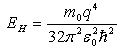 which is equal to 13.6eV. The ionization energy of Ed could be replaced
with the above formula by changing the rest mass to effective mass of electrons for conductivity and the dielectric permittivity
by semiconductor permittivity, which is equal to 13.6eV. The ionization energy of Ed could be replaced
with the above formula by changing the rest mass to effective mass of electrons for conductivity and the dielectric permittivity
by semiconductor permittivity, 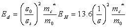 . These ionization energy which values may not give all the details,
such as deeper energy levels of semiconductors, but they do give the order of the values. . These ionization energy which values may not give all the details,
such as deeper energy levels of semiconductors, but they do give the order of the values.
|
| |
| |
| |
| |
| 2.2.2 p-type doping |
| |
Group III of periodic table elements is suitable for p-type doping. They are Boron, Gallium and Indium so on. The outermost shell contains three electrons, if such elements replace a Silicon atom; one bonding remains vacant, see fig2.8(c). Hence the dopant is ready to accept one electron and thus called an Acceptor. The Acceptor energy level are close to valence band (see fig 2.29). Typical ionization energies of acceptors and donors for Silicon are given in the above table.
|
| |
|
Fig 2.28(a)Electron bound to a donor does not contribute to the conduction.
But when(b) the donor is ionised, electron becomes free and hence
contributes to the charge transport .
|
| |
| Donor energy levels (E d ) in eV |
Acceptor energy levels (E a ) in eV |
As= 0.054 ; P= 0.045
Sb= 0.043 |
Al= 0.072 ; B= 0.045
Ga= 0.074 ; In=0.157 |
|
| |
| |
| |
|
Fig.2.29. Schematic energy diagram of (A) n-type and (B) p type doped semiconductor
|
| |
| |
| |
| |
| |
| 2.2.3 Densities of carriers in extrinsic semiconductors and their temperature dependence |
| |
|
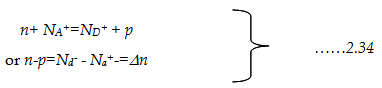
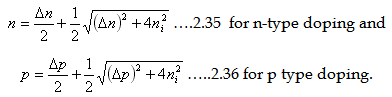
In n- type semiconductors electrons are majority carriers and holes are minority carriers. Whereas, in p-type semiconductors holes are the majority carriers and electrons are minority carriers. We studied earlier that the electron and hole densities are exactly equal in intrinsic semiconductors, but now we will see what happens to carrier concentrations if acceptors (or donors) are added to intrinsic semiconductors. We know the expression for intrinsic carrier concentration from Eq.2.28 as ni2 = n0.p0 =Nc.Nv exp(-Eg ⁄ kT . n0 and p0 represent carrier concentrations of electrons and holes in an intrinsic semiconductor. When the dopants are added, the Fermi level must readjust to attain charge neutrality, which means that the total electrons must be equal to the total holes.
To preserve such neutrality, assuming both acceptors and donors are added,
n+ NA+=ND+ + p.
.2.31
NA-, ND+ indicates densities of fully ionized acceptors and donors.
At very low temperatures only few donors are ionized and majority is bounded to the parent ion. As the temperature gradually increases donors starts ionizing and the electrons are transported into the conduction band (Fig 2.28). At a certain temperature, all the donor atoms are completely ionized
(
Nd=Nd+). The expression for the ionized donors with respect to temperature is
|
| |
where g is the degeneracy factor (value is 2 which means it accepts both the spins).
|
Similarly the expression for ionized acceptors is
|
| |
Where the degeneracy factor value is 4, which means it accepts one of the other spin and they doubly degenerate due to valence band degeneracy.
If both acceptor and donors are present, then, according to the charge neutrality,
|
| |
| |
We know that at thermal equilibrium, the product of electrons and holes are equal to intrinsic
density ni2 , that is (n0p0=ni2). Just solving the n-p and np from the above expressions,
we can easily arrive at the carrier concentration expressions
|
| |
| |
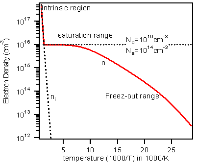
If we plot carrier concentration (combining Eq.2.32 and Eq.2.35 for donors) with respect
to temperature for a given donor impurity densities (ND), we will observe many things.
Let us assume donor and acceptor impurities are 1016cm-3 and 1014cm-3 respectively ( Nd>>Na) ,in Silicon.
Typical carrier concentration vs temperature (in terms of 1⁄T) graph is as shown in figure (2.30). As you can see,
the carrier concentration response of the extrinsic semiconductor can be divided into three regions:
(1) Freeze-out zone,
(2) Saturation (or extrinsic or operating) region and
(3) Intrinsic region.
|
| |
|
Fig.2.30. Electron density as a function of temperature in Silicon.
The parameters are Nd=1016 and Na=1014 cm-3, both Ed and Ea are 50meV,
the activation energy equal to 27.4 meV at 70K
|
| |
| (1) Freeze-out region: |
Near to temperatures at 0K, the electron density is zero and all electrons (within semiconductor) are in
lowest possible states, which mean they are bound to the parent ion ( refer to fig 2.28). As we increase the temperature donor atoms
slowly get ionized, and as a result the electrons travel from donor level (Ed) to the conduction band. This phenomenon is called Freeze-out.
This will continue until all the donors are completely ionized and this can typically lead up to 150K. The electron density is smaller than
the donor density since only the impurity atoms are ionized. This region is called freeze-out region. Note that here the carrier concentration
greater than that of intrinsic carrier concentration.
|
| |
| (2) Extrinsic Region: |
Above ~150K, all the electrons are completely ionized so that n=ND.
This region is called extrinsic region. This region extends to little beyond room temperature and most
of the devices works in this region only. Here the electron density is completely dominated by the minority
carriers. It is also interesting for you to note, say at room temperature the extrinsic carrier concentration
is exactly equal to dopant concentration (in our case it is 1016cm3) and will be constant over a range of temperatures.
For a comparison, intrinsic silicon carrier concentration, at this temperature is only 1.5x1010cm-3, which is about six
orders less than extrinsic carrier concentration!.
|
| (3) Intrinsic Region: |
After that, the intrinsic carrier concentration rapidly increases and eventually
it reaches greater than Nd.
Now the carrier concentration is fully dominated by majority change carriers. Now, a large number of electrons are thermally excited from valence band and the semiconductor behaves much like intrinsic, that’s why the region is called an intrinsic region.
|
| |
| |
| |
| |
| |
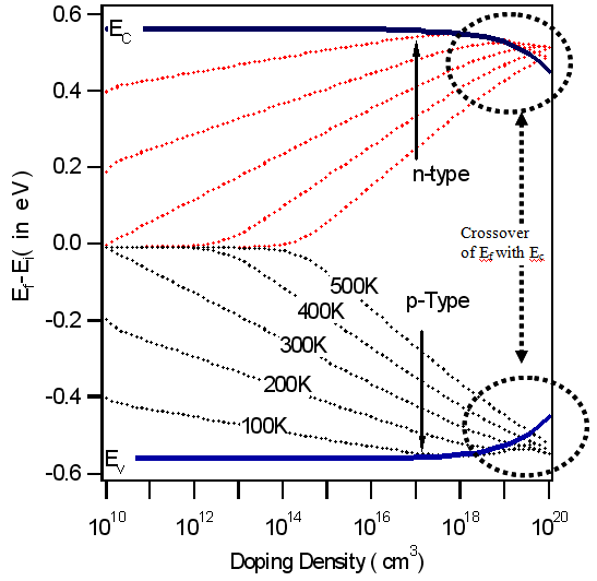
| 2.2.4 Fermi Energy level of Extrinsic semiconductors |
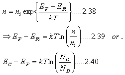
Now let us examine the Fermi energy level of extrinsic semiconductor.
If we recall our discussion of Fermi levels, the Fermi energy level in the intrinsic semiconductor lies approximately halfway in between
conduction and valance bands (Ei=(EV+Ec)⁄2). Also recall the Eq. 2.26 and 2.27 for electron and hole density equation as a
function of Fermi level.
Let us re-write the expression
|
| |
which ultimately can be represented as
|
| |
Where EF and EFi stands for Fermi levels of extrinsic and intrinsic semiconductors
respectively.
Fermi level in n type semiconductor 
|
| |
and for p- type it is
|
|
| |
This suggests that in n-type semiconductors, Fermi level (EF) is higher than Ei and close to the
conduction band. Similarly, in p-type it moves down towards the valance band (see Fig.2.31). The location of Fermi level in
extrinsic semiconductors is useful to know, for device applications, which we will see more in our forthcoming chapters.
|
| |
|
Fig 2.31 . Fermi energy of doped silicon ( n type and p type)
vary with doping density as well as temperature. As the temperature ( doping) increases Fermi level shifts towards
conduction band (Ec) in the case of n-type doping and shifts towards valance band ( Ev) in p-type doping.
( observe where Fermi level crosses Conduction (valance) band!)
|
| |
| |
| |
| |
| |
| |
| |
| |