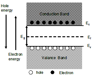
Fig2.19: Electron- Hole concept
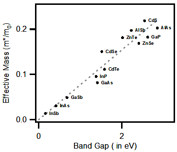
Fig.2.20. Variation of effective mass with band gap energy of different semiconductors.
Now it is clear here that the electron and hole numbers are equal. But if we make either one of them more, what happens? That we will see in our later parts.
 for electrons and
  for hole.
Here one important thing : the conduction band effective mass is directly related to the band gap energy Eg. The smaller is the band gap, the smaller is the effective mass (Fig.2.20). Here you can observe some interesting points: for example see band gap is decreasing in the alloys CdS, CdSe and CdTe ( You know why?). Similarly AlAs, GaAs and InAs.
The band gaps of few semiconductors at the room temperature are given in the table. However, with the temperature the band gap substantially varies. This is shown graphically in fig 2.21. The empirical relation of band gap vs temperature is
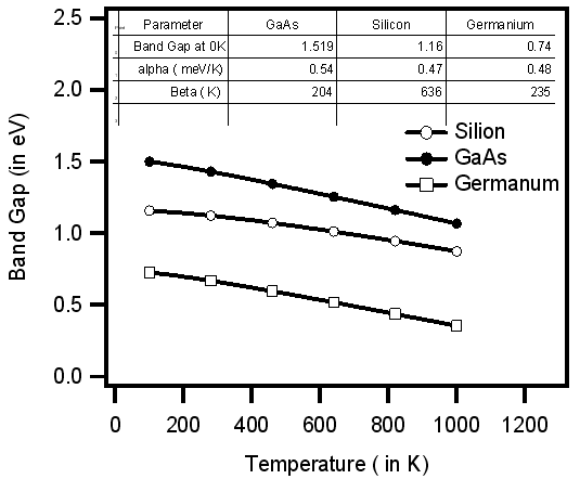
Fig. 2.21. Temperature dependence of Band gap of some of the important semiconductors.
As we know that the energy bands are a mix of energy levels of individual atoms of the semiconductor. With the help of Schrödinger’s equation (through sophisticated mathematical algorithms) electron motion can be solved and one can obtain energy–momentum relation or simply, E-k band diagram. Though, throughout our semiconductor physics class, we are mostly interested in the energy levels at the top of the valence band and bottom of the conduction band, which lie in the vicinity of the band edge. However, every semiconductor has uniquely had its own band structure. As we observed earlier, semiconductors can be broadly divided into direct band gap and indirect band gap semiconductors, depending on the conduction band minimum position with respect to valence band maximum. As schematically represented in figure 2.22, we can see two kinds of conduction minima ( one at k=0 and another at k≠0). Similarly, at valance maximum we can see two closely connected bands (or curves) namely, Heavy Hole (HH) Light Hole (LH), and one at little far called Split-off (SO) .
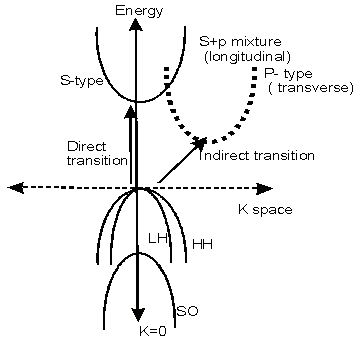
Fig. 2.22. Valance and conduction band type in typical semiconductor
- In the direct band gap materials central band of electrons at the conduction band is purely s-type.
- In the indirect band gap materials conduction band is either s and p mixture (longitudinal) or p type (transverse).
- In silicon, the bottom of the conduction band does not occur at k=0 but at six equivalent minima long, kx, ky and kz directions ( look at those BZ points in Fig 2.9). For Si, there are six equivalent points (2Π/a)(0.85,0,0), (2Π/a)(0,0.85,0), (2Π/a)(0,0,0.85), and inverse of these three, where a is the lattice constant of Si (=5.430A)
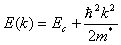
- Simple way of representing direct band conduction energy( in parabolic representation) is
 . For indirect band, generalized conduction energy
is along a particular axis is
. For indirect band, generalized conduction energy
is along a particular axis is 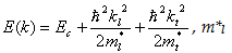 and m*t stands for longitudinal and transverse effective masses.
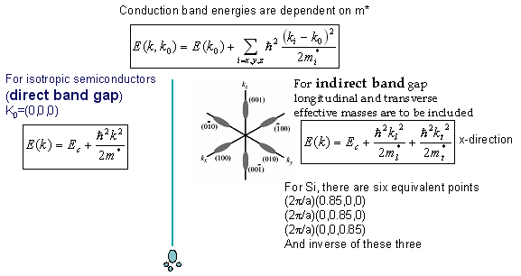
Figure: Notice six equivalent points for the conduction band minima in Si along the crystallographic axes
 , and
, and These energy states could be generally represented as
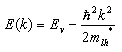
Where A, B, C and D are dimensionless parameters. +ve and ve signs represent heavy hole (HH) and light hole (LH) states. Corresponding to HH and LH states, effective masses of electrons in the conduction band also vary. Unlike conduction band, for both direct and indirect bandgap materials, the effective mass of valance band is defined as for both kinds of materials.
Table 1.5.1
| Property | GaAs | Silicon | Germanium |
| Conduction band | |||
| Band Gap (eV) | 1.42* (d), 1.73(I) | 3.2(d), 1.12*(I) | 0.8(d), 0.66*(I) |
| Effective mass (/m0 ) | 0.067d, 1.98(l) and 0.37(t) |
0.2d, 0.98(l) and 019(t) |
0.04d, 1.64(l) and 0.08(t) |
| Valance band | |||
| HH Effective mass(/m 0) | 0.45 | 0.49 | 0.28 |
| LH Effective mass(/m 0) | 0.08 | 0.16 | 0.44 |
| SO Effective mass(/m0 ) | 0.15 | 0.29 | 0.08 |
|
|||
Effective mass- Density of states
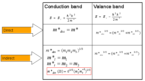
Table 1.5.2
| Property | GaAs | Silicon | Germanium |
| Lowest band gap (eV) | 1.42 | 1.12 | 0.66 |
| Electron effective mass (for DOS)(/m0 ) | 0.06 | 1.08 | 0.55 |
| Hole effective mass (for DOS)(/m 0) | 0.45 | 0.81 | 0.37 |
| Electron effective mass (for Conductivity)(/m 0) | 0.067 | 0.26 | 0.12 |
| Hole effective mass (for Conductivity)(/m0 ) | 0.34 | 0.39 | 0.21 |
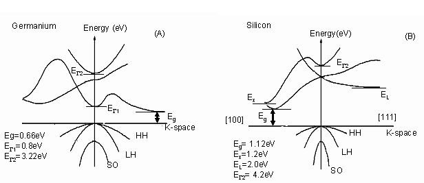
Fig 2.23 Band diagram(E vs k) (A) Ge (B) Si, where high-lying energy bands also shown.