| Fundamental concepts of semiconductors |
| |
| |
| Introduction |
| |
Semiconductors fundamentals, in general, are explained by quantum mechanical and statistical thermodynamics. This chapter aims to introduce the concepts of bands, origin, and the electron behavior
in various bands with or without external influence.
We shall introduce various concepts in brief, however, it is with a belief that the reader might have had a minimum background in the solid-state basics and quantum theory.
|
Precisely, we treat the semiconductor as a crystalline material, consisting of atoms arranged in a highly
ordered pattern, called lattice (we shall discuss this little later). Though all materials may not be necessarily crystalline
(could be either quasi crystalline or amorphous), but in the short-range or at the microscopic level, they are crystalline.
Once we treat the lattice as a periodic potential, we see remarkable properties that explain the physical nature of semiconductors.
This chapter contains the information on how the atoms are arranged and how the electrons behave in the lattice, which helps to understand the properties of semiconductor. We will also discuss the concept of electrons and holes and how their occupancy probability alters the properties of semiconductors. Finally, we will see the transport mechanisms of charge carriers, which eventually come under the drift and diffusion processes.
|
| |
| |
| |
| 1.2 Crystal structures |
| |
| Although some materials are disordered, many can be understood from the fact that the atoms
are periodically arranged. So instead of thinking about 1023 atoms/cm3, one can think about few atoms, together
with the underlying symmetry of the crystal. For the moment we are going to assume that the crystals are not infinite and they do not have any defects in them, because we can add these back later. |
| |
| The first part of our formalism is to divide the structure into the lattice and the basis. |
| |
| The lattice is an infinite array of points arranged in space so that each point has identical surroundings.
This means, you can go to any lattice point and it will have the same environment as the others.
The basis means atoms attached to each lattice point. |
| |
| Nearest neighbor lattice points are separated from each other by the 3 fundamental translation
vectors of the particular 3-dimensional lattice, which we generally write as a, b and c.
Then any of the lattice points are linked by a lattice vector given by: |
| |
T = n1 a + n2 b + n3 c (where n1, n2, n3 are integers)
|
 ( this is the arrangment in 2D) ( this is the arrangment in 2D)
|
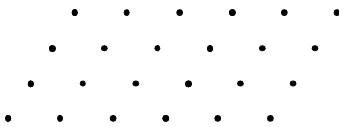
| Fig 2.1 Schematic view of 2D lattice |
| |
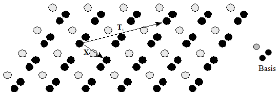
| The basis of the crystal has been just the specific arrangement of atoms attached to each lattice point.
So, for instance, we can have a three atom basis attached to the above lattice (fig 2.1) to give the crystal structure
as shown in the fig 2.2. |
| |
| Moving by any lattice vector (e.g. T1)
takes to a position, which looks perfectly identical. This reflects the translational symmetry of the crystal. |
| |
Note that X is not a lattice vector, as the shift it produces results in a different atomic environment,
refer to fig2.2a. Most elements have a small number of atoms in the basis, such as silicon, which has two,
whereas Mn has a basis with 29 atoms! Compounds will have a basis with more than one element,
e.g. CaF2 has one Ca atom and two F atoms in its basis.
|
|
Fig 2.2a Two dimensional representation of lattice and basis, indicating the lattice vector
|
| |
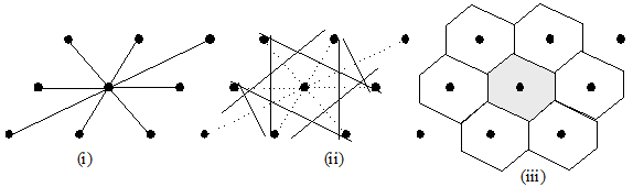
| We often talk about the primitive cell of a lattice, which is the volume associated with a single lattice point.
You can find the primitive cell using the following procedure: |
| |
- Draw lattice vectors from one lattice point to all adjacent lattice points
- Construct planes normal to the above vectors which divide the vectors by half.
- Find the volume around the lattice point enclosed by these planes.
|
| |
|
Fig. 2.2b: Construction of the Wigner-Seitz cell (identical to the first Brillouin zone in the
reciprocal lattice). First draw lines to the nearest
neighbourhood
(2)draw perpendicular bisectors and the area enclosed is
now called as first WS cell. (iii) Each atom is now enclosed by its WS cell..
|
| |
This type of primitive cell is called a Wigner-Seitz cell (fig2.2b), but other ones are possible
with the same volume (or area in the 2D case), and which can be tiled to fill up all of the space. As seen in figure 2.2b,
fist figure represents the real space lattice
and figure (iii)
represents a unit cell contained in the reciprocal space with a specific name, Wigner-Seitz cell or the first Brillouin zone.
|
| |
|
| |
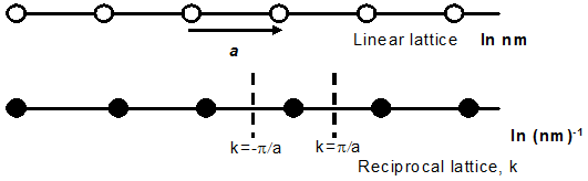
Fig.2.3. Linear and reciprocal lattice in one dimension. The basic dimension of linear lattice
is a, whereas reciprocal lattice is 2 π/a. The perpendicular bisector boundaries are ± π/a (Brillouin zone boundaries).
|
| |
Similarly, one can also draw WS cell, as shown infig2.3, in reciprocal lattice which is of
great importance for solid-state physicists. Particularly, they are of more use in the analysis of energy-band
structures and we will be looking into this very soon..
|
| |
An electron in a crystal can be treated as free or nearly free electron with a well
defined momentum, characterized by the wave vector k. As the electron motion in real space is very poorly defined,
it is far easier and appropriate to describe the electron in momentum (k) space or reciprocal space. Always, the crystal
structure is associated with two lattices, the real crystal lattice and the reciprocal lattice.
|
| |
|
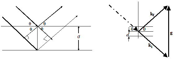
Fig.2.4 (a) Bragg diffraction by a lattice of atoms treated as an array of planes
(b) Geometry of diffraction with incident & diffracted wavevectors ( of 2π/λ) and the reciprocal
lattice vector g (of 2 π/a)
|
| |
If the basic dimension of linear lattice is a, then the reciprocal lattice dimension is 2π/a.
|
| |
The relation between the reciprocal lattice vector g to the real lattice vector R is defined as g.R=2πn. Where n is an integer.
Recalling your memory on Braggs diffraction, reflecting a wave from an object which scatters and has periodicity
(such as a lattice of atoms) gives rise to strong diffracted waves in specific directions (which you briefly covered
in your previous classes ). We can assume each plane reflects light (mirror-like), and the array of stacked planes gives
rise to interference between these reflections. The path difference between the reflection from successive planes are given
by AB+BC=2dsinθ. Where d is the spacing between the planes ( for us it is lattice constant a).
For constructive interference (Fig2.4a) this must be a whole number of wavelengths, giving the Bragg law condition,
2a.sinθ=nλ and Δk.a=2πn. Where Δk is the difference between
the wave vectors of the incident ray and reflected ray
and θ is the angle
between them. This suggests that the constructive interference when the phase difference ( between incident and
reflected ray) is integral multiples of 2 π. The vectors, whose magnitude is equal to the half of the
reciprocal lattice vector, from the surface of the first Brillouin zone. That means if the unit cell magnitude in
reciprocal space is 2π/a,
magnitude of the
k vector is equal to the π/a. As you have seen from fig. 2.2,fig. 2.3, first
Brillouin zone in 2D and 1D, for 3D it is more complex than you imagine.
|
| |
| |
Although some materials are disordered, many can be understood from the fact that the atoms
are periodically arranged.
As stated earlier, we shall ignore the defects in the crystals. In this course, we are not going to attempt any exhaustive survey of crystal structures, and would restrict to only cubic systems.
The reason is that there are 32 classes of
crystals with four types of unit cells. What we will do here is to introduce a formalism because it will help us
to understand the structure and other related properties in a powerful way.
|
| |
|
| |
Fig. 2.5 (a) Simple Cubic, (b) body centered cubic (bcc) and (c) Face centered cubic (fcc) crystal
|
| |
| |
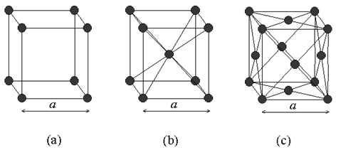
As mentioned before, a crystal is defined as basis plus lattice. Among all crystal types
cubic class of crystals is of much importance in semiconductors. Cubic crystal contains three different
varieties, depending on the atomic arrangement (Fig 2.5) : simple cubic, body-centered cubic (BCC) and face-centered
cubic (FCC) . Simple cubic contains atoms at each corner (total eight), however eight other unit cells share each atom.
Therefore, eight corner atoms effectively contribute one atom to the unit cell. Both BCC and FCC are
formed by adding extra lattice points to the unit cell, either in the center of the cell or at the center of each
face of the cube respectively (see Figure 2.5). The cubic unit cell is then no longer primitive, but is still more
convenient to work with.
|
| |
see more crystal structures at http://cst-www.nrl.navy.mil/lattice/ and http://www.cryst.ehu.es/
|
Interestingly, the reciprocal lattice of a simple cubic is again a simple cubic.
Whereas reciprocal lattice of a body centered cubic (bcc) is a face centered cubic (fcc) and The reciprocal
lattice of a face centered cubic (fcc) is a body centered cubic (bcc). (You want to show how? try)
|
| |
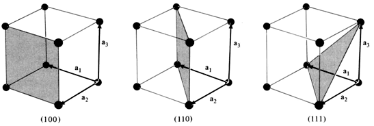
Another important representation is to identify individual planes
or surfaces of the crystal. Surfaces or the planes through the crystal are described by considering the intercepts of
the planes along x,y and z coordinates. Look at the specific example (Fig2.6), the lattice planes are shown along axes only.
Atoms are arranged in 3D space and say the intercepts for the respective axes are 3, 2 and 1.
The reciprocal of the intercepts is therefore (1⁄3 ,1⁄2 , 1⁄1), by multiplying with the common denominator (which 6) we obtain
(2, 3, 6). This means the plane in the figure (2.6) represent the lattice plane referred to (2, 3, 6).
These integers are well known as Miller indices and are generally represented as (h,k,l). Miller indices of important planes
of a cubic cell are given given in figure 2.7, |
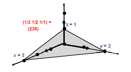
Fig. 2.6 Representative of crystal lattice plane. |
| |
|
| |
Fig 2.7. Three lattice planes, (100), (110) and (111) plane.
|
We can also show that the same miller indices planes are obtained for any plane
parallel to the one shown in the figure 2.7 have the same miller indices of that plane.
|
| |
| Let us do a simple problem to understand more about unit cell. |
| |
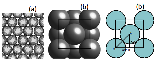
Naturally-assembled spheres tend to form a periodic crystalline structure of face
centered cubic (FCC) symmetry. However from the top view they look like hexagonal! Let us find out if the cubic
cell width is a, the packing fraction. (Packing fraction is defined as number of spheres (or atoms) in the cell
multiplied by volume of a sphere (atom) divided by volume of the unit cell)
The closely packed hard spheres are as given in figure2.5. Here the right side a cubic face (b and c) view is given where,
you can see the sphere appears in the middle of the face. The lattice constant a is now 2OB (see figure 2.5 c). Considering triangle OAB,
the radius of the sphere is just OA/2 that is √2 a/4 .
|
| |
|
| |
Figure Top view of closely packed spheres (hexagonal),
but in fact, they form closely packed fcc (b). (100) plane view is as given in (c).
|
| |
Now let us calculate the sphere arrangement and their sharing in the fcc unit cell.
|
- Each corner is shared by 1/8thof a sphere and for 8 corners total spheres contributed to the unit cell is one.
- Each face is shared by 1/2thof a sphere that is 6 faces totals to 3 spheres which contributes to the unit cell.
|
So the total number of spheres in the fcc unit cell is (3+1=4 spheres).
|
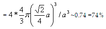
Packing fraction= (no. of spheres per cell) * (volume of a sphere) / (volume of the unit cell)
|
|
Similarly, we can calculate volume density (No. of atoms/volume) and surface density for each plane
(No. of atoms per plane/area of the plane).
|
| |
|
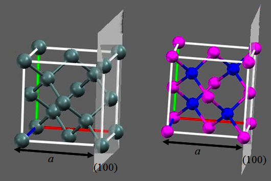
Fig.2.8a. Diamond lattice of Si, Ge ;
(b) Zinc-blende structure of GaAs and InP (Blue represents Ga/As and pink for As/Ga respectively)
|
| |
|
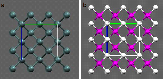
Fig 2.8b. 2-D representation of (a) silicon and
(b) III-V(eg: GaAs) semiconductors along a( or b or c) plane. Note the way in which group III and V atoms are alternatively
attached to each other through their lattice on their individual FCC sub-lattices
|
| |
For Example, in simple cubic lattice there is just one atom at 000.
|
body centre cubic lattice (bcc) the atomic positions are 000, 1/21/21/2.
|
face centre cubic lattice (fcc) the atomic positions are 000, 01/21/2, 1/201/2, 1/21/20.
|
| |
Let us look at some real semiconductors: Silicon (Si) is the most common semiconductor that represents a diamond
like crystal structure. It is simple to understand as an FCC structure with additional four atoms embedded inside the unit cell (Figure 2.8a).
Similar is the case for another important group IV element Germanium (Ge).
|
Interestingly, another important binary alloy Gallium Arsenide (GaAs), slightly differs from diamond
structure (Fig 2.8a), which is called as Zinc Blende (after another semiconductor ZnO) structure. The difference between the diamond structure
to the zinc Blende structure is that, the atoms embedded inside the FCC are different in Zinc Blende Structure. In our GaAs, the FCC structure formed by As (or Ga)
atoms and four Ga ( or As) atoms are now embedded inside the FCC lattice.
|
| |
Unlike Si, in the group III-V semiconductors, a group III atom is bonded to four group V nearest atoms,
similarly group V atom bonded to four group III nearest atoms (Fig2.8b). It is also interesting to see
that Si unit cell is having symmetry while GaAs does not ( because of different atoms inside). This explains many property differences,
such as light emitting and nonlinear optical phenomena, between Si and GaAs.
|
| |
|
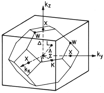
Fig. 2.9. Some important symmetry points in FCC crystal (diamond and zinc-blende lattices).
If a is the lattice constant then the symmetry points are : Γ point : kx=ky=kz=0; X point: kx=2π/a, ky=kz=0;
and L point: kx=ky=kz= π/a
|
| |
| |
| 1.2.1 Rules for band representation: |
| |
We have learned previously how to draw BZ planes for 1D and 2D. In 3D the same procedure is followed except
the lines are now planes and the enclosed area becomes volume. The sketch of the first BZ of FCC lattice is given in figure 2.9. Very important
to remember, BZ volume is associated in k-space and representation of directions are important in dealing energy band diagrams. Directions are
chosen in such a way that they lead from the center of the Brillouin zones in the more generalized to special symmetry points. These points are
labeled according to standard notations:
|
| |
- Points (and lines) inside the BZ are denoted by Greek letters.
- Points on the surface of the BZ are denoted by Roman letters.
|
| |
- The center of the BZ (k=0) in the reciprocal lattice is always denoted by Γ
- The intersection point with the [100] direction is called X (H); the line Γ X is called Δ.
- The intersection point with the [110] direction is called K (N); the line Γ K is called Σ.
- The intersection point with the [111] direction is called L (P); the line Γ L is called Λ.
|
| |
|
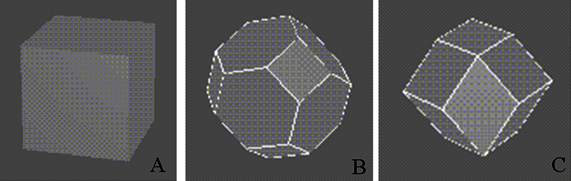
Fig. 2.10. Three dimensional representation of First Brillouin zone of (A) simple cubic,
(B) Face centered (FCC) and (C) body centered (BCC) cubic crystals, in the reciprocal lattice.
|
| |
Let us see now how the reciprocal space or k space is important for getting band information of crystals.
We know that the vectors whose magnitude is equal to exactly half of the reciprocal lattice vector from the surface of the first Brillouin zone
. If the lattice constant is a, then the reciprocal lattice is 2Π/a. Hence half of it is simply Π/a.
|
| |
Assume the incident and reflected ray wave functions of electron are 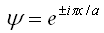 (+ and are for incident and reflected respectively), where the electron k vector is Π/a. (+ and are for incident and reflected respectively), where the electron k vector is Π/a.
Consider the situation in which the linear combination is equal to the amplitude.
Hence the combinations are
Ψ(+) or Ψ(-) respectively are
|

|
| The probability densities (ρ) are the square of electronic wave function. Thus,
we have two probability density functions for both
|

|
| If you observe closely, by applying boundary conditions x=0 and x=a, electron most likely to be
found at x=a for Ψ(+) function, that is near to the center. At the same time for Ψ(-) it is zero.
|
| |
So, as a conclusion we can say that, near
one Brillouin zone
edge, k=Π/a, the band structure under goes
a discontinuity in the energy spectrum, suggesting the band gap.
It is now clear to us why the knowledge of Brillouin zones
important, since it defines all k vectors for which Bragg reflection occurs.
|
However, in reality, band theory is more complex than it seems to be.
There are broadly two approaches to find the electron energies associated with atoms in a periodic lattice.
Method 1: Unbound or Free Electron Approach where free electrons are modified by a periodic potential (i.e. lattice ions).
Method 2: Bound Electron Approach Isolated atoms brought close together to form a solid.
|
Note that both the approaches result in grouped energy levels with allowed and forbidden energy regions.
The theory is generalized for all materials (i.e) metals, semiconductors and insulators. Just to recall, metal energy levels are strongly
overlapped, while for semiconductor and insulators they have defined gap in the energy, where finding an electron is forbidden.
|
| |
| |
| |
| |
| |
| |
| |
| |