| Introduction :Fundamental concepts of semiconductors |
| |
| |
| |
| 1.1 Introduction |
| |
Semiconductor devices make modern information technology possible. One can imagine, the semiconductor industry
is much more profitable than steel industry, with sales of more than $200 billion market in the US!! (2005 statistics).
One would also accept that the present generation is driven by information and communication: where semiconductor
devices are most critical components.
But what makes a semiconductor so important? |
| |
Let us list out some of the key points of semiconductor applications: |
- The Wide choice to alter the physical properties (example: high to low electrical resistivity,optical materials covering from UV to far infrared applications).
- Ultra-fast response times .
- Multi-functional (source, operation and
detection) devices
- Tailoring opportunity, in such a way that the device allows to implement all sorts of information processing.
- Boolean logics, signal amplifiers, store and retrieve information, processing, light source
many more.
|
| |
| What is the real advantage in learning about semiconductor? |
| |
| Here are some of the examples of semiconductor related careers. |
| |
Table 1.1.1 |
| Examples of Careers |
- Lasers and Optoelectronics :
Designing new laser diode sources Medical, industrial laser applications; laser micromachining
|
Creation of novel "smart" or "self-assembling materials ,Satellite/aerospace materials
|
- Nanotechnologies and Devices :
Development of new microscopes- Atomic Force Microscope Micromachined and silicon integrated Microphones(MEMS related)
"Lab on a Chip", nanobiotechnology Nanotechnology process engineer, Quantum computing, Ion thrusters for rocket propulsion
|
- Fluids, Mechanical Engineering, Biomedical Engineering: :
Controlling turbulence in oil pipelines, microfluidic devices Design of artificial limbs Magnetic Resonance Imaging
|
- Electronics : Electronics:
Build and test CCD detector arrays for remote sensing Custom electronics design for systems/devices
|
Microdevice fabrication simulation , Laser fusion modeling
|
| |
University professors, college instructors, high school teachers
|
|
| |
| Where are the semiconductor stands in the list of materials? |
| |
Table 1.1.2 |
| Metal |
Semiconductor |
Insulator |
| Silver, platinum copper gold.. etc |
Silicon, Germanium, etc., |
Teflon, Quartz, SiO2 etc., |
| Conductivity : 106 to 1 (Ω-m)-1 |
10-8 to 103 |
10-7- 10-25 |
| Highest occupied energy bands are partially filled with electrons: |
Completely filled at low temperatures. Upper band conduction band is empty |
|
|
| |
| |
| |
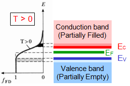
| Metals: |
| |
Highest occupied energy bands are partially filled with electrons, while above the Fermi energy level(EF)
all bands are empty. With a very small amount of energy lead the electrons go to the conduction band, leading to high conductivity.
At T>0 electrons thermally excited and cross the barrier of EF .
|
| |
 |
| |
| Insulators: |
| |
At T=0 Conduction band is completely empty and valence band is filled, leading to zero conductivity.
Very big energy gap (Eg>4,5 eV)between conduction (EC) and Valance (EV ) bands, where EF is in the middle.
No thermal excitation and hence even higher temperature, conduction are zero.
|
| |
 |
| |
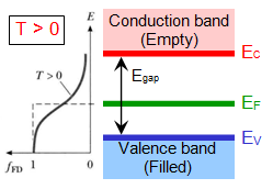
| Semiconductors: |
| |
At T=0, conduction band is empty and valence is completely filled, hence zero conductivity. Eg is < 4eV( Si: 1.17, Ge=0.74, GaAs= 1.52eV at T=0).
At higher temperature electron thermal excitation does happen and hence the conductivity lies between metal and insulator.
|
|
| |
| |
Table 1.1.3 |
| |
Group II |
Group III |
Group IV |
Group V |
Group VI |
| |
|
B |
C |
N |
|
| |
|
Al |
Si |
P |
S |
| |
Zn |
Ga |
Ge |
As |
Se |
| |
Cd |
In |
|
|
|
|
| |
| |
In general, any material property varies typically according to the electronic configuration.
If we look into the periodic table, the group elements in a column have similar properties, gradually changing from top to
bottom. Mostly, the electrons are in the outmost shell govern most of the physical properties.
Our Semiconductors occupy some of the III to IV columns in the periodic table and they could be a mix of
various combinations called alloys.
|
| |
One of the uniqueness of semiconductor is that the properties can be widely tailored,
according to our requirement, by simply modifying the alloy combinations. Apart from this, we can also add a small fraction of other
materials, so called doping, and change the properties. The best example is doping in Si. We can change the property of Silicon
to electron rich (n-type) or deficient (p-type) by adding(doping) Boron or Phosphorous atoms respectively.
|
| |
Some of the important Semiconductors and their combinations (alloys) are
|
| |
Table 1.1.4 |
| Elemental |
IV alloys |
III-V binary alloys |
II-VI binary |
Ternary alloys |
Si, Ge
|
SiC,
SiGe
|
Al Y (Y=P,As,Sb),
GaY(Y=N,P,As,Sb)
IY(Y=P,As,Sb) |
ZnX, CdX
(X=S, Se and Te)
|
AlGaAs,
|
|
| |
Another important aspect in learning these material characteristics is how atoms are arranged.
They can be either crystalline ( well-ordered), amorphous (disordered) or polycrystalline ( short range order).
|
| |
However, we are probably still at the beginning stages of the microelectronics age.
Though several properties of semiconductors to control electrical and optical features to make these materials
much useful for electronic and photonic devices, the strive for the best is still going on. These properties include,
electrical resistivity and optical absorption, which are related to one another. Significantly, these properties depend on the
molecular-scale structure, the atom positions and the electron states around these atoms. One of the scientists from
the UK commented in an interview to the BBC
channel
in 2001, about the competition in the scientific world.
|
"This was the new level of science that you had to match yourself up against, and everybody knew they couldn't,
they couldn't meet that. It was almost like competing against a god really."
|
| |
| |
| |