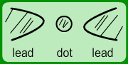
A typical semiconductor device utilizes many electron; for example there can be 1011 – 1012 electrons in 1 cm2 area of a typical MOSFET device, so that even an area as small as 1 μm x 1 μm involve 103 – 104 electrons. On the other hand, if a device size well below 0.1 μm is achieved, then a single electron may be involved in the device application, where the concept of coulomb blockade plays an important role. This is based on the following observations: when an electron is transferred from lead to the small system (e.g., quantum dot) then there is a rearrangement of charge in the lead, resulting in a change in the electrostatic potential energy (see Fig. 8.1). |