| |
It is also possible to obtain an Ohmic contact between a metal and a semiconductor that would normally form a Schottky diode, such as a metal for which
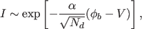
 . For such a contact, usually a heavy inhomogeneous doping (called graded doping) close to the interface is employed to achieve large barrier height having very narrow barrier width, as shown schematically in Fig. 4.20. In such a case, the main mechanism of carrier transport is tunneling through the narrow barrier (a topic to be dealt with later). The tunneling current is |
|
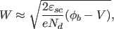
where  is the depletion layer width which can be approximated as |
|
| so that |
|
where
 . |
|
|
|