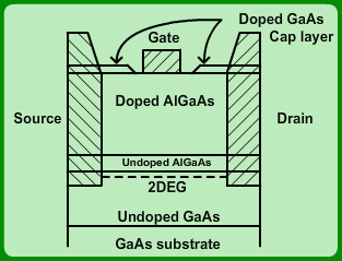
In this structure as shown in Fig 2.6, a layer of unintentionally doped GaAs (typically with carrier density between 1014 to 1015 cm−3) is grown on a semi insulating GaAs substrate. Then an undoped space layer of AlGaAs is grown followed by a thicker heavily doped layer of AlGaAs. A cap layer of doped or undoped GaAs is usually grown on top for ohmic contact and to reduce oxidation of AlGaAs layer. Since the free carriers forming a channel at the GaAs /AlGaAs interface are spatially remote from their parent donors, ionized impurity scattering is greatly reduced, and mobilities in excess of 1017 cm2/ (V.s) are attainable in such structures. |